 In this post, you can see the design of a little low-voltage universal LED flasher. The flasher is in fact a standalone module but it can also be used with most 3.3V (or 5V) microcontrollers – that is to say, just another universal microcontroller-compatible design which is more lenient and flexible too!
A simplified schematic of the universal low-voltage flasher is shown in the figure below.
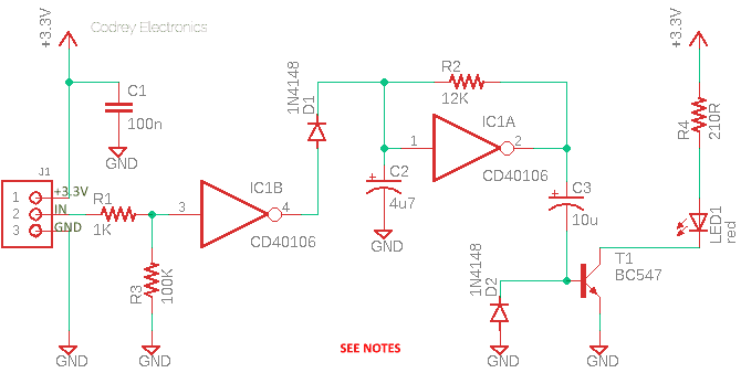
In this circuit, a basic relaxation oscillator is constructed with the first gate (IC1A) of the Schmitt-trigger inverter CD40106BE (IC1). The frequency of oscillation is approximately equal to 9Hz which is set by the RC timing components R2 and C2.
The second gate (IC1B) of IC1 is used to ‘gate’ the IC1A oscillator through a 1N4148 diode (D1). A logic-high level TTL signal (3.3V) at IC1B’s input will ‘enable’ the relaxation oscillator IC1A because IC1B is merely a logic ‘inverter’ that outputs the opposite logic level from what’s put in. If the input sees a high voltage level, it sets the output low, and vice-versa.
The final output stage of the circuitry has a BC547 transistor (T1), a 10uF decoupling capacitor (C3), 1N4148 diode (D2), LED1, and a current limiting resistor (R4) to provide a visual indication of the low-frequency relaxation oscillator operation. A 5mm red LED is preferred here, you can use another type/colour though.
As you can see in its datasheet, the CD40106BE is a hex inverter with ‘hysteresis’. It’s a good pick for our ‘universal’ idea because it’ll work on a wide voltage range – 3V is a fair minimum. Now look over the schematic for a second and note that there’s two vital things that you have to do. First, the unused inputs of IC1 should ideally be connected to ground, that means grounding pins 5, 9 11, and 13. Second, hook up power rails to pins 14 (+3.3V) and 7 (GND) of IC1.
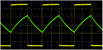
Now note that this circuit relies on hysteresis to make the oscillator run. The input (Pin 1) of the oscillator (IC1A) sees the capacitor (C2) charging and discharging between the two threshold levels. Since the output voltage is constant and the voltage on the capacitor is increasing over time, the current that flows through the resistor (R2) drops a little during the cycle, so the result is a triangle wave that’s made out of exponential curves rather than straight lines. And, as soon as the voltage on C2 reaches the relevant threshold, the output (Pin 2) toggles its state, and the final outcome then is a square wave that bounces between two logic voltage levels.
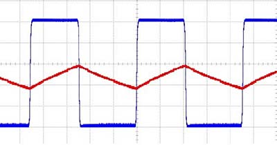
Following is a casual oscillogram taken while my breadboard setup is powered by a regulated 3VDC input. Here the upper trace (yellow) is the IC1A output (Pin 2), and the lower trace (green) is its input (Pin 1).
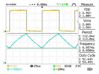
And, here is what it looks like when the output (Pin 2) is extended to the final driver stage through the 10uF capacitor (C3). Here the right trace is the IC1A output (Pin 2), and the left trace is its input (Pin 1). An oscillogram is worth a thousand words, yeh?
Enough lecture. It’s time for you to build yours!
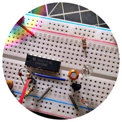
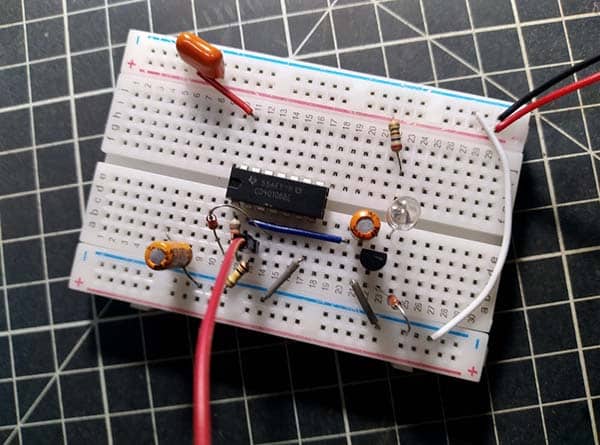
When you’re building along, it’s good to test this out on the breadboard at first, and maybe try to build a perfboard version or whatever later. Below is a snap of my nearly-finished breadboard assembly. I used a 5mm blue LED for LED1 and provided the requisite 3V trigger input through the 1K resistor R1. Don’t forget to watch out for the quick test movie included at end.
Needless to say, the given circuitry will work happily with 5V microcontrollers too, provided its power supply input is 5VDC. The frequency of oscillation, however, changes with the power supply voltage, mind it!
So, by now you’ve got something built up on your workbench that can be used either as a standalone LED flasher, or a microcontroller-switchable LED flasher module. Nevertheless, now it starts to get more interesting because you’ve got four ‘spare’ inverter gates, any of which could be used to enhance the simple idea I’ve putting out so far.
Finally, if this little project motivates you to pick up some nostalgic stuff that’s lying around unconsidered for much too long, then I’ve got a bunch more pragmatic ideas coming up for the next installments of this ‘old school’ series. See you then!

What will happen if we supply logic low level signal at 1C1B input pin..
Shubhneesh Sangwan: As you can see in the schematic (and clearly mentioned in the text), the relaxation oscillator is inactive in normal state because the input of IC1B is pulled low via pull-down resistor R3. So, if you give a logic-low signal input nothing will happen. Simply, a logic-high level TTL signal (3.3V) at IC1B’s input wakes the relaxation oscillator up!
Thanks for the Reply.. I just asked because in this circuit (link to circuit) LED2 blinks when output OUT1 of the MCU is low and glows constantly when the output is high. Could you please explain how the LED is changing it’s blinking state when we change the logic at OUT1 from HIGH TO LOW or LOW TO HIGH ..
Shubhneesh Sangwan: When referring to that link provided, you may contact its author through the site for further clarification.
Regarding my post, I’m sure the explanation is enough. Else, you just study the CD40106 datasheet to learn more about hex inverters and their functions!
Link to Circuit….
https://www.electronicsforu.com/electronics-projects/efficient-led-blinking-for-embedded-systems#:~:text=The%20frequency%20of%20blinking%20is,when%20output%20OUT0%20is%20low.