 A while ago, I designed a Power MOSFET Load Switch circuit using a handful of components that I use in little power electronics projects to allow a regular slide switch to control power on/off function. I am sure someone else has done something similar (or a step advanced) before, but it was fun figuring it out for myself. Okay, check out its schematic below.
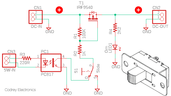
This minuscule circuit is an alternative to beefy power on/off switches as it uses a small slide switch to control a high-side power MOSFET that can be useful for applications at power dissipation levels to approximately 50W. The circuit also has an integrated photocoupler which makes it easy to control the MOSFET with a galvanically-isolated external signal or the digital output of a microcontroller. Moreover, since the main current does not go through the mechanical slide switch/photocoupler, a variety of switches/photocouplers can be used without concern for the current they can handle!
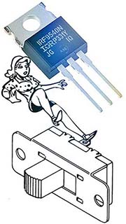
As it seems, the key part in this circuit, designed primarily for 12VDC operation, is the IRF9540 P-channel Power MOSFET (T1). In the most common application, power can be applied to the CN1 connector (DC-IN), with the slide switch controlling power on the CN2 connector (DC-OUT). To use an external signal to control T1, set the slide switch (S1) to the off position and then feed the control signal through the third 2-pin connector CN3 (SW-IN).
Note that the aforesaid 2-pin connectors do not have reverse polarity input protection features, so the dc voltage and the external control signal should be inputted to the circuit with correct +/- polarity. Further, you may need to change the value of the photocoupler’s current limiter resistor R3 (220Ω default) when you want to use a “strange” external control signal.
Load Switch Basics & Design Considerations
A load switch is comprised of two main elements – the pass transistor and the on/off control mechanism as shown in my schematic. The pass transistor is most commonly a MOSFET (either N-channel or P-channel) that passes the voltage supply to a specified load when the transistor is on. The choice of a P-channel or N-channel MOSFET actually depends on the specific needs of the proposed application. The P-channel MOSFET however has a distinct advantage over the N-channel MOSFET, and that is in the simplicity of the on/off control mechanism. The N-channel MOSFET requires an additional voltage rail for the gate (The P-channel MOSFET does not).
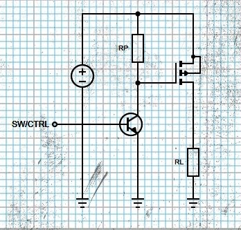
The above figure shows an example load switch circuit with a P-channel Power MOSFET. Here, an external switch/control signal turns the MOSFET on and off via a small-signal transistor. When the switch/control input is LOW, the small signal transistor is off and the MOSFET’s gate is pulled up to VIN. But when the switch/control input is HIGH, the small-signal transistor turns on, the MOSFET gate is pulled down, and it turns on. As long as the input voltage rail is higher than the threshold voltage of the MOSFET, it will turn on when the switch/control input is HIGH without the need of an additional voltage source. The “pull-up” resistor is selected so that milliamps of current or less flow through it when the small signal transistor is on (The standard range is 1K to 10KΩ).
To put it simply, a MOSFET can be treated as a variable resistor whose Drain-Source resistance (Rds) is a function of the voltage difference on the Gate-Source pins (Vgs). If there is no potential difference between the Gate-Source, then the Drain-Source resistance is very high and so no current flows through the pins. On the other hand, if there is an appropriate Gate-Source voltage, the Drain-Source resistance is very low and acts as a closed switch thus current flows through the pins.
At this point, it’s worthy to take note that because the MOSFET in its on state is effectively resistive, the power heating it is proportional to the square of the current flowing through it (I2). Nevertheless, with proper cooling (or for brief periods if it is not hot to begin with), currents up to the recommended maximum is come-at-able.
The load switch MOSFET (pass transistor) must have a continuous current rating greater than the maximum load current of the proposed application. Likewise, the MOSFET must not be operated outside of its specifications. Operation outside of the specified region can degrade the performance, reliability, and lifetime of the MOSFET, and can potentially ruin other components within the circuitry.
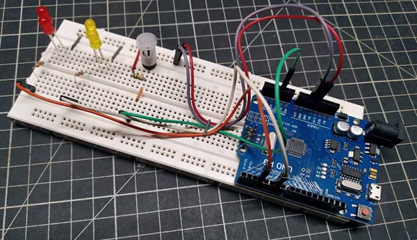
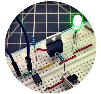
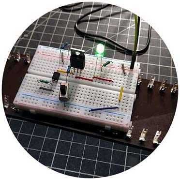
Going back to my project, I would like to say that my first prototype was on a mini breadboard. I intend to continue working through the improvements and will post updates as appropriate. If you are interested in additional details, including design decisions and calculations use the comments box to simply throw something in my way!
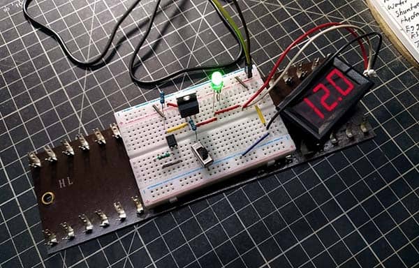
The image shown is my first breadboard prototype. Later I slightly modified the design (that is the schematic provided in the beginning) and finally set it on a small circuit board. That final build has proven its worth in various hobby projects so far.
Finally, this has been a short post and only scratches the surface. I hope this will be a starting point for further exploration into solid-state load switch designs.
Quick Reference https://www.rohm.com/electronics-basics/transistors/what-is-a-load-switch