The Arduino is an excellent microcontroller you probably already know that. An Arduino board can however only control low-current devices, so often you need a proper driver circuitry to handle the low-current control signals and drive the high-current devices. Today, I will share a couple of random thoughts on how to enhance the power-driving capability of your Arduino designs.
Driver based on a BJT
A common task for a transistor is switching a device on and off. As a driver, the BJT (bipolar junction transistor) operates in saturation mode, means there’s enough base current to turn on the transistor fully. To use a BJT as a driver, you need to know several things to be successful – for example, current requirement of the load (Ic), and gain of the transistor (hFE). Then you can calculate the base current (Ib) to find the right base resistor.
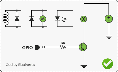
Well, just assume that the load (incandescent bulb) in this circuit requires 100mA of current, and the NPN transistor picked out has a typical gain (hFE) of 110. Then, the base current is 100/110 = 0.909mA. Since the output voltage of an Arduino GPIO is 5V in logic-high state, the base resistor (RB in the above schematic) value is 5 – 0.7/0.909= 4730Ω. For such a feeble current and small voltage, one 4.7KΩ ¼ W resistor is fine. If the circuit is used to drive inductive loads such as coils or motors, it must be equipped with a diode to damp the inductive driver-off back-emf.
Here, the load is between Vcc and the transistor, and the transistor is wired to ground. Since the transistor is switching the path to ground i.e. resting on the low side of the load, this configuration is called as a “low-side driver”. The opposite of this is the “high-side driver” where the transistor is wired between Vcc and the load.
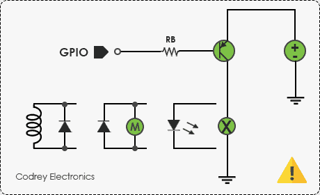
Just note that the dc current per GPIO (aka I/O) pin of an Arduino (5VDC) is 40mA. When using the PNP transistor based circuit similar to the one provided below on a load voltage that is the same voltage level of the GPIO of the microcontroller, it works fine (ofcourse the logic-level is inverted). However, if the load voltage is higher than that, it’s extremely risky to try high-side driver configuration.
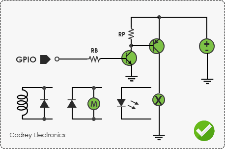
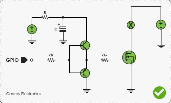
Below you can see an improved version of the PNP transistor based high-side driver. This is actually a very common configuration where an extra NPN transistor is used to drive the PNP transistor. This configuration is an effective solution when you have a load that requires ‘true’ ground.
Driver based on a MOSFET
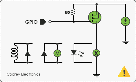
A MOSFET offers a number of advantages over a BJT. Now I’ll show you both ways to build a MOSFET based driver/driver. The first circuit shown below uses an N-channel MOSFET, and the second one is a P-channel MOSFET based circuit. Remember, the location of the MOSFET determines the circuit type and its name.
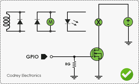
Obviously, a high current MOSFET’s has a substantial Vgs threshold. Since the 5V output from an Arduino GPIO pin might not be adequate to turn on the MOSFET, a ‘logic-level’ MOSFET is required in this N-channel MOSFET driver circuit.
Now to an improved version of the P-channel MOSFET based high-side driver. once more, an additional NPN transistor is used here to drive the P-channel MOSFET.
There you have it, however, this is only a mere introduction. There’re literally innumerous web articles explain about this topic, so don’t stop here!
Isolated Power Driver
An isolated power driver can provide safe galvanic-isolation between the microcontroller GPIO and the power driver/switch circuitry. This is especially useful if the target circuit uses a higher supply voltage, as using GPIO pins to drive other devices directly could be potentially dangerous in many situations. Fortunately, it’s quite easy to rig up an isolated power driver/switch. Let’s see how.
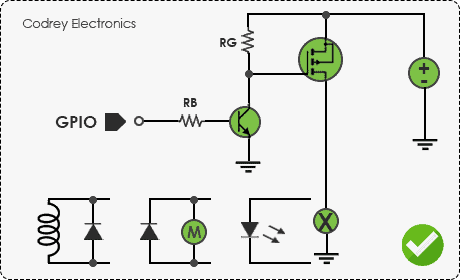
Following is a simplest circuit of an isolated power driver wired around an N-channel MOSFET. Here, signal from the GPIO pin of the microcontroller drives the ‘sender’ segment of the optocoupler. Arduino GPIO pin can render at least a few mA current so driving the optocoupler directly via a current limiting resistor should not be an issue. The ‘receiver’ segment of the optocoupler is used for turning the MOSFET on and off. Note that the circuits on either side of the optocoupler do not have to share a common ground reference – fully isolated, yup!
You can ofcourse use an NPN BJT in lieu of the N-channel MOSFET in this scheme but in most applications the MOSFET has some distinct advantages over the BJT.
Switching Time – BJT & MOSFET
For transistor switching times, the switching speed of the device can be a significant quantity. See, when the base input current is applied to a BJT, it does not switch on immediately because the switching time is influenced by junction capacitance and the transit time of electrons across the junctions. The time between the application of the input pulse and beginning of collector current flow is termed the delay time (td).
Even when the BJT commences to switch on, a finite time elapses before collector current (Ic) reaches its maximum level. This is called as the rise time (tr) which is specified as the time required for collector current to go from 10% to 90% of its maximum level. So, the turn-on time (ton), is the sum of delay time and rise time.
Likewise, when the base input current is switched off, collector current does not go back to zero until after a turn-off time (toff), made up of a storage time (ts), and a fall time (tf). The fall time is specified as the time needed for collector current to go from 90% to 10% of its maximum level.
Therefore, the ton and toff of the BJT used in your ‘fast switching’ power driver circuit must be of the order of nanoseconds (ns).
When it comes to MOSFET switching times, it’s important to optimize the MOSFET switching speed by adjusting the gate resistor value. Generally, a resistor is wired to the gate terminal of a MOSFET for suppression of inrush current and a reduction in output ringing.
Keep note that the gate of the MOSFET looks like a capacitor to the source. The gate voltage of a MOSFET does not increase unless its gate input capacitance is charged, and the MOSFET does not turn on until its gate voltage reaches the gate threshold voltage. The gate threshold voltage(Vth) of a MOSFET is specified as the minimum gate bias required for creating a conduction channel between its source and drain regions. An in-depth explanation is omitted on this session, and it’s intentional. For further reading/learning, you can checkout these links https://octopart.com/blog/archives/2018/06/fast-switching-semiconductors-selecting-power-mosfets , https://www.infineon.com/dgdl/mosfet.pdf ,
https://www.infineon.com/dgdl/mosfet.pdf
Switching Time – Optocoupler
As stated earlier, the main purpose of an optocoupler interface is to completely isolate the input circuit from the output circuit, which normally means there will be two completely separate power supplies, one for the input circuit and one for the output. The simplest form of optocoupler consisting of an infrared LED and an infrared phototransistor with a black plastic shell that shields its internal opto-electronics.
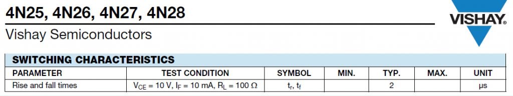
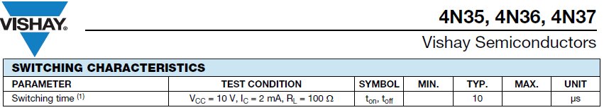
However, phototransistors are generally not as fast as photodiodes at reacting to abrupt changes in light levels. In principle, the time taken for the phototransistor output to change between 10% and 90% in response to a sudden change in light level at the input is a bit higher than that of a high- speed photodiode. Manufacturers usually quote these figures for rise time (tr) and fall time (tf) under particular conditions (see below).
Put simply, while using an isolated driver in a pulse width modulation (PWM) circuit, keep an eye on the speed of the optocoupler used there, and ensure that the minimum pulse width of the PWM signal must be longer than the switching speed of the optocoupler.
If you know the frequency of the PWM (Fpwm ) and the rise time (tr) and fall time (tf ) of the optocoupler, a quick calculation can be made to get the number of discrete steps that the optocoupler can accommodate. Formula: n = 2/[Fpwm (tr +tf )]
For example, if the combined rise and fall times of the selected optocoupler is 10uS, then the optocoupler can see a maximum of 400 steps at a PWM frequency of 500Hz. An 8-bit PWM yields 256 steps (28) and since the optocoupler can attain up to 400 steps, these parameters might work together.
On a side note, pins 3,5,6, 9, 10,11 of Arduino Uno can be configured for PWM output. The 8-bit PWM value that you set when you call the analogWrite function. If you use the default values, these are your PWM frequencies – Arduino Pins D9, D10, D11, and D3 = 500Hz, and Arduino pins D5 and D6 = 1kHz.
Driver based on a MOSFET – More Thoughts
A MOSFET is normally thought of as a voltage controlled device, decent voltage at the gate drives the MOSFET and lets a large current to flow through the drain/source. A MOSFET is indeed an efficient switch but only when completely on or off, because it’s inefficient when switching and dispels losing as heat. This calls for a clever gate driving technique, and it becomes particularly crucial while switching the MOSFET on and off quickly with a PWM signal.
One solution advised by the experts is to use a bipolar totem-pole driver. The idea behind that is that by using the very fast operation and large gain of bipolar transistors the gate can be charged and discharged quickly. Lets take a look at the basic scheme of such a bipolar totem-pole driver.
Here, when the PWM signal is high the NPN transistor is on and the PNP transistor is off. This allows a large current to flow into the gate of the MOSFET. And, when the PWM signal is low the PNP transistor is on and the NPN transistor is off allowing for a quick sink of the charge on the MOSFET gate into ground. That certainly works nice.
MOSFET Driver IC – Why & When?
Digital signals are meant to drive small loads usually on the order of 10-100pF, while bigger MOSFETs have higher gate capacitance which can be in the thousands of pF. Also many large MOSFETs have a higher gate voltage, naturally above the logic-level output provided by the GPIO pin of a microcontroller. Moreover, there’s another (overlooked) issue – switching MOSFET can cause a back-current from the gate back to the driving circuit. MOSFET drivers are designed to handle this back current, too.
Absolutely, a MOSFET driver chip translates a logic-level signal to a higher voltage and higher current adequate for rapidly and completely switching the gate of a power MOSFET. While choosing a gate driver, make sure that its output voltage capability has to be match the turn on voltage of the power MOSFET.
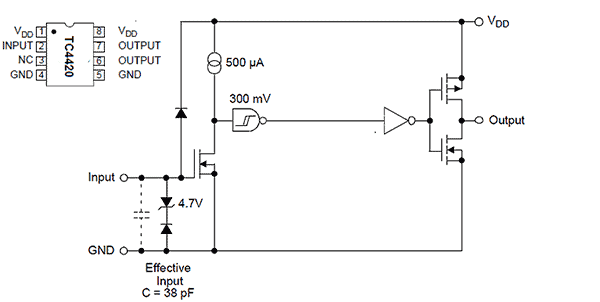
Below you can find the functional block diagram of TC4420 (6A, high-speed, non-inverting) MOSFET driver IC from Microchip Technology Inc.
Next is about a real-world test. Now I’m preparing two versions of a MOSFET based 10W-20W LED driver for the succeeding part of my previously posted “LED strobe Light DIY” project (https://www.codrey.com/electronic-circuits/led-strobe-light-diy/). My first idea is based on the dedicated high-speed power MOSFET driver chip TC4420, and the second version is centered on the TC4427 dual high-speed power MOSFET driver chip (yet to be gathered). Stay tuned…
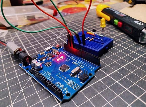
In the meantime, you can try this code to build a simple interleaved pulse width modulation generator with an Arduino Uno.
/* Interleaved PWM Generator  with an Arduino Uno */

int PWM1 = 0;
int PWM2 = 0;

void setup() {
TCNT1 = 0x7FFF;
pinMode(9, OUTPUT); // PWM O/P Channel 1 = D9
pinMode(11, OUTPUT); // PWM O/P Channel 2 = D11
}

void loop() {
delay(500); //500ms delay
analogWrite(9, PWM1);
analogWrite(11, PWM2);
PWM1++; // Increment PWM1
PWM2++; // Increment PWM2
}
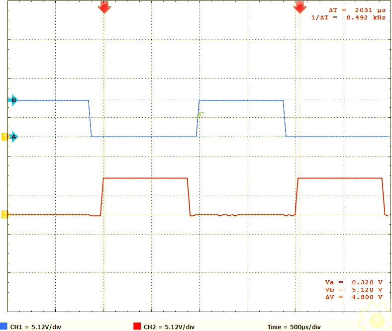
This is a cursory oscillogram of the resultant:
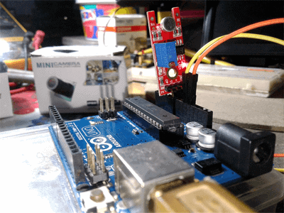
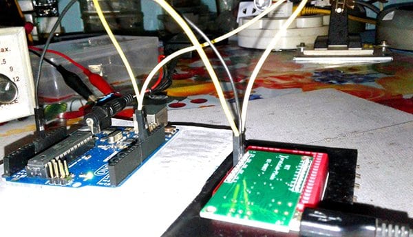
And, this is a snap of the test setup:
This adaptable setup is useful for many different experiments including testing of high-power driver circuit ideas discussed in this post. As there is a lot of information already published here on pulse width modulation for the Arduino, I didn’t go into too much this time. Please feel free to ask questions and I’ll do the best I can to answer it. I hope this helps some people out there!