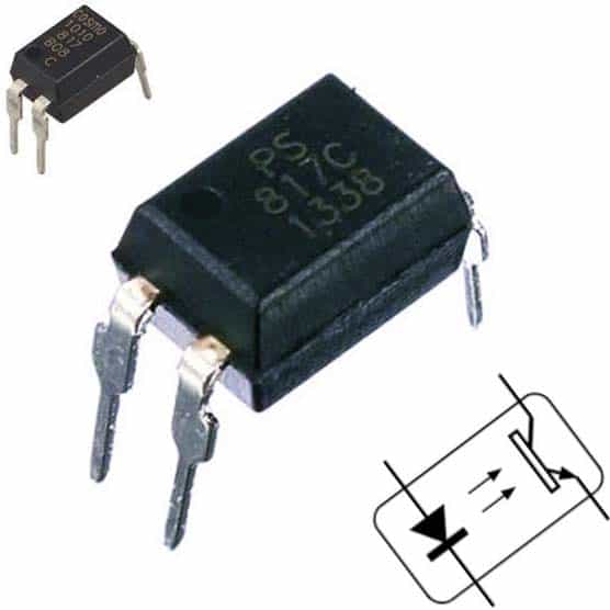
An optocoupler, simply put, is a little device consisting of an independently-powered light transmitter and light receiver unit packed inside a light-proof shell that can be optically coupled together. Actually optocouplers are very easy to use devices, with the input side being used in the fashion of a normal light emitting diode and the output used in the fashion of a normal phototransistor. In normal use, operating current of the internal light emitting diode is limited via an externally connected series resistor which can be wired on either the anode or the cathode side of the light emitting diode. Optocouplers can be used as either input or output devices.
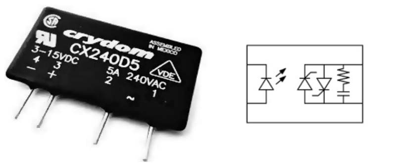
The solid state relay (SSR) is in fact a bit beefy variant of the regular optocoupler as it also provides complete galvanic isolation between its input and output segments thru an optically-coupled mechanism. Its output, however, acts like an electrical switch that has a very high resistance when open and a very low resistance when closed, and in closed state the output circuit can pass AC or DC well.
Sometimes, you will need a simple and safe adapter circuit for optocouplers and solid state relays in a rather serious microcontroller based setup with potentially long cables. In such situations, a constant current source controlled by the microcontroller would be a clever pick.
Below is the schematic of such a constant current source tailored for optocouplers and solid state relays. This is a very simplistic and relatively inexpensive implementation that uses a jellybean NPN transistor as the key element – the constant current generator!
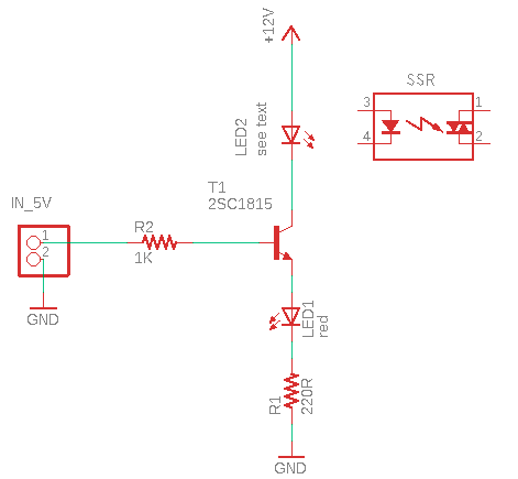
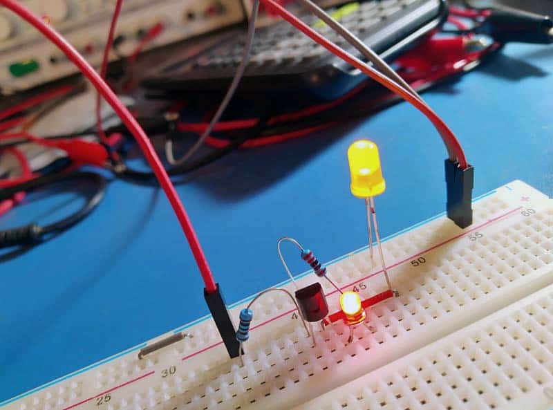
This circuit is designed to be work with a 12V dc (9V-12V) power source. The control signal at its input (IN_5V) could be as simple as a 5V TTL or CMOS logic signal without a current limiting resistor in series. The red LED is there to provide a perceptible visual indication.
This simple circuit strictly follows the textbook concept of the NPN BJT constant current source. That is, just keeping a constant voltage at the base of the 2SC1815 transistor (T1) to get a constant voltage at its emitter. The 220Ω resistor (R1) wired from the emitter of T1 to ground rail (GND) ensures a constant emitter current, and this is nearly the collector current. So, no matter what is connected at the collector, it will “see” the same current.
In other words, transistor T1’s base voltage and emitter resistor R1 set the current. The emitter voltage, roughly 600mV less than the base voltage, is held across the emitter resistor, and collector of T1 will pass the whatever current is needed to hold the voltage across the emitter resistor. Here it is around 10.6mA with the 220Ω emitter resistor.
It is of import to note that in reality, this setup does not behave like an ideal source where the current is fixed. Two different effects have to be considered:
- hFE (Early effect) varies with VCE
- VBE and hFE vary with the temperature
Side note: The Early effect, named after its discoverer James M. Early, is the variation in the effective width of the base in a bipolar junction transistor (BJT) due to a variation in the applied base-to-collector voltage.
Also, the load current is constant only if the voltage is such as to guarantee that the BJT works in the active region.
Back to the show, now note that in my breadboard mock up, a 5mm yellow LED (LED2) is connected on the collector side to imitate the optocoupler/solid state relay load as it induces a voltage drop close to 2V (VF =2V @ 10mA).
Finally, this circuit is not part of any projects so far but I assume it could compete well in reality. Even trivial concepts like these bear a great potential of optimization. Depending on your demands, sometimes a few milliamperes do not matter but in certain cases you may need it to be a bit more precise. So, go make your better mousetrap…