So, I am revisiting emitter follower this moment and sharing my dusted thoughts on it. I hope this post helps someone one way or another!
This article mainly looks at an emitter-follower (also known as voltage follower) circuit based on a common NPN transistor. Needless to say, a good discernment of the emitter followers’ properties (and operation) will help electronics lovers from many different disciplines.
Look, in a transistor emitter follower circuit, the voltage at the emitter follows the input voltage. It is a mirror image, so to speak, of the input voltage. Therefore, the voltage at the output is roughly the same as the voltage at the input. Since the configuration has a high input impedance and a low output impedance, it can act as a buffer. An emitter follower is generally used as a voltage buffer and helps drive loads.
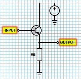
Concisely, the emitter follower uses a fixed collector voltage for the transistor, and the output is at the emitter. Every change in the input voltage means that the emitter voltage is automatically chased, as even a very feeble base-emitter differential voltage is enough to change the emitter current significantly. The voltage amplification is almost unity, that is to say, the input voltage is not amplified, but the input current is.
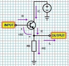
The theoretical input impedance ZIN here will be β x RE, so with an emitter resistance of 1KΩ and a current gain of 200, this simply results in 200KΩ.
An eagle-eyed reader will have noticed at this point that since the base-emitter junction of a transistor is also a diode, it will always maintain approximately the same voltage across itself regardless of the current flowing through it. For a silicon BJT, this is around 650mV so the output voltage on the emitter will always be 650mV lower than the input voltage on the base. Okay, here the output voltage follows the input voltage but is shifted down by VBE (0.6V to 0.7V) , and thus the gain will always be just a bit less than unity.
Another key point to make is that an emitter follower (common collector) circuit can be used as an AC-coupled linear amplifier by biasing its base to a quiescent half-supply voltage value to accommodate maximal signal swings, and AC-coupling the input signal to its base and taking the output signal from its emitter. This means that there is a demand for an output coupling capacitor to block the DC component, and often, an input AC-coupling capacitor will also be required particularly if the source has a DC potential.
So, a textbook emitter follower circuit with a single NPN BJT is shown below. The BJT that is chosen can really be any regular transistor – at this time it is a 2N3904 transistor.
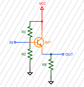
Then to the values of the components used. Note that some approximations are made when choosing the resistor values (rounded up or down to the nearest standard values).
- BJT = 2N3904
- R1 = 15KΩ
- R2 = 22KΩ
- RE = 1.2KΩ
My design math was based on the following assumptions:
- VCC = 12VDC
- BJT Beta = 150 (based on the specifications in the transistor datasheet)
- BJT VBE = 700mV (typical voltage between base and emitter of the transistor)
- Quiescent Collector Current = 5mA (just a safe value, that is it)
- Signal Source Impedance = 50Ω
I will not go over the calculations, but want to note that this snippet helped me a little https://physicscourses.colorado.edu/phys3330/phys3330_sp16/Labs/PHYS3330_lab7_sp16.pdf
So, the AC input resistance of this circuit, as counted, is around 8.5KΩ and the AC output resistance is 5Ω (http://www.guitarscience.net/calcs/cc.htm). However, be aware that the given circuit is in its crude form i.e. it is not optimised for any particular application.
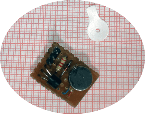
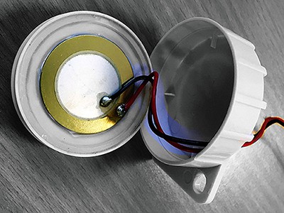
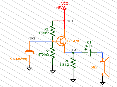
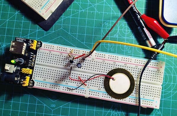
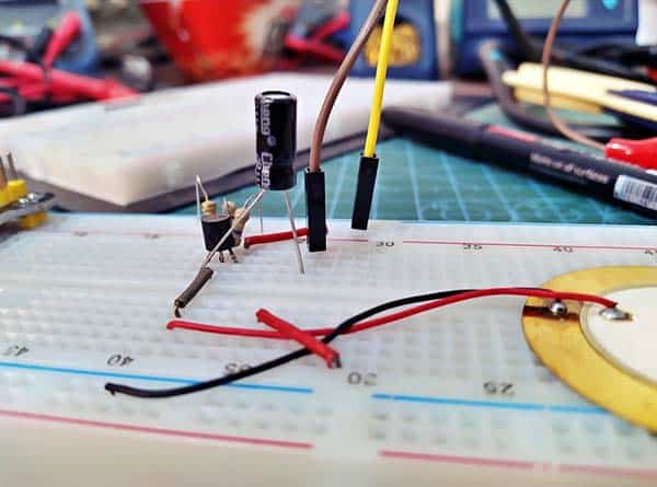
But below you can see a simple practical circuit of the emitter follower. With this circuit, a piezoceramic sound transducer (piezoceramic disc) can be used as a contact microphone to capture structure-borne sound waves. At the output you just need to plug a low impedance earphone to be able to listen to the mystic grumbles. Give it a try.
Be aware that piezo transducers need to work at high impedance. This circuit works as an impedance converter to buffer the piezo transducer. Strictly speaking, it does not inevitably boost the signal, but it matches the output impedance of the piezo transducer to the input impedance of the device at the output.
Also note that piezoelectric elements are capacitive, which means their impedance is inversely proportional to frequency. The resonance of a piezo disc however can be reduced by increasing the mass of the disc. A proven scheme is to increase the mass of the metallic part, while not overly loading the central ceramic portion (more on this later).
Well, below is a casual snap of my breadboard mock up with a regulated 5VDC breadboard power supply.
The voltages at the various test points shown in the schematic above are listed below.
- TP1: 4.99V
- TP2: 1.92V
- TP3: 1.32V
As an interim conclusion, I think this spry writing has been somewhat successful in sharing the flakes of a complex topic in a transparently clear manner. But this is just the beginning and there will be more discussion on this in a later post. I hope to get some feedbacks as well!