Today, let us have a quick look at the task of boosting dc voltages.
It is perhaps worth noting that every other consumer electronic gadget on the market performs some form of voltage conversions imply because the voltage we get out of a typical battery or another power source is seldom right for every part of the circuit.
Buck/Boost Converter
Touching on inductor-based dc-dc voltage converters, a buck converter is usually used to get a tightly-controlled output voltage lower than the input supply, and to generate a higher output voltage, the most common route is the so-called boost converter topology.
Boost Converter Basics
The operation of a boost converter circuit is fairly straightforward. Anyway, I will provide a brief explanation here.
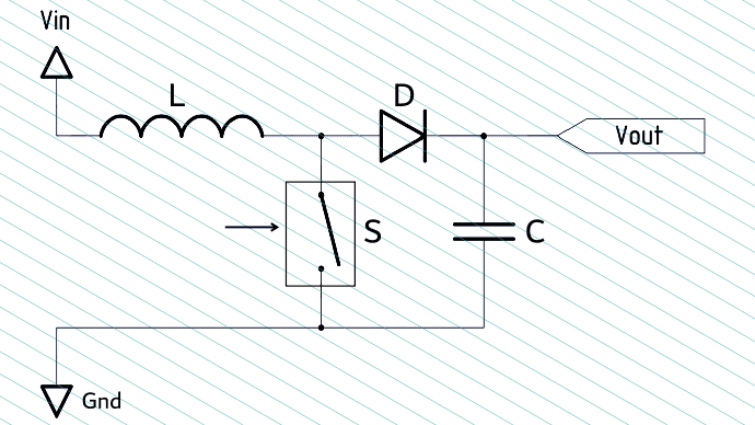
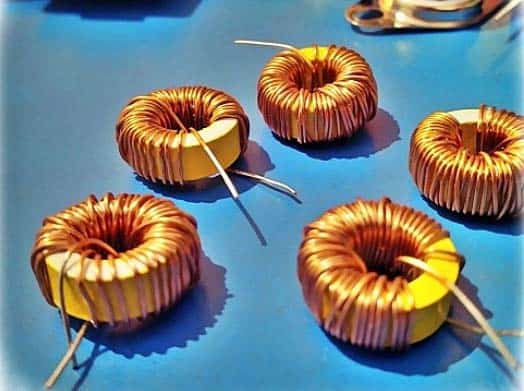
In the above depicted basic boost converter architecture, closing of the switch (S) creates a short-circuit between the supply rails – but for a brief while, the inductor (L) resists the flow of current while diverting the energy of the supply into an internal magnetic field (this effect fizzles rapidly, so to avoid a real short-circuit, the switch needs to be opened before long).
Once that circuit path is broken, the collapsing magnetic field of the inductor tries to sustain the flow of charges in the direction they were flowing before, and this pushes the left terminal (input point) of the inductor more negative, and makes its right terminal (output point) more positive.
Note, however, that the left terminal of the inductor side is still connected to the positive supply rail (Vin), so its potential remains constant in relation to the supply; meanwhile, a dc voltmeter connected to the other terminal would show a voltage higher than the input voltage (Vin). This voltage spike causes the diode (D) to start conducting, letting energy transfer to the output capacitor (C), thus the output capacitor can be charged to a higher voltage as well. Finally, the critical output voltage (Vout) regulation can be achieved by varying the ‘on’ time (→) of the inductor.
To make this concept more practical, the switch can be replaced with a power mosfet as shown in the below figure. Here, a high frequency square wave signal is used to switch (on/off) the power mosfet.
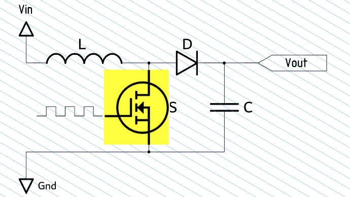
At this point, during the time the mosfet conducts, a short circuit is created between the righthand side of L to the Gnd terminal. Therefore a current flows between the Vin and Gnd rails, which stores energy in its magnetic field. There is virtually no current flowing in the remainder of the circuit as it represents a much higher impedance than the path directly through the mosfet.
On the flip side, when the mosfet is rapidly turned off ,the sudden drop in current causes L to produce a back-emf (BEMF) in the opposite polarity to the voltage across L during the mosfet on time, to keep current flowing. This results in two voltages, the supply voltage Vin and the back-emf across L in series with each other.
This higher voltage (Vin+BEMF), now that there is no current path through the mosfet, forward biases the diode D. The resulting current through D charges up C to Vin+BEMF (minus a small forward voltage drop across the diode), and also renders the output (Vout).
So, a dc-dc boost converter is an electronic circuit whose output voltage is greater than the input voltage. It consists of at least one semiconductor switch and a combination of an inductor, a rectifier diode, and a buffer capacitor. The boost converter then boosts the input voltage and gives it to the output load.
Of course, the pulses needed to drive the semiconductor switch can be generated in many ways. I could not have said it better – a detailed explanation is given on Wikipedia.
Well, now if you want to obtain the output voltage depending on the input voltage and the duty cycle of the switching waveform all you have to do is to make the sum of the on and off current equal to 0. That means that the on current is equal to the off current.
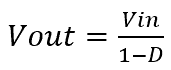
So, the theoretic dc output voltage (Vout) of the boost converter is determined by the input voltage (Vin) divided by 1 minus the duty cycle (D) of the switching waveform (which will be some figure between 0 and 1, corresponding to 0 to 100% duty cycle) and therefore can be determined using the following formula:
Note at this point that the output voltage is dependent on the switching waveform duty cycle, so it is important that it should be accurately controlled (the bigger the duty cycle beats, the higher will be the output voltage).
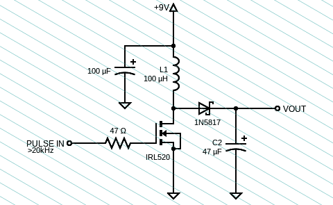
Boost Converter Homework
Frankly, the below boost converter example/experimental circuit has no sense but to learn.
In order to make it 5V TTL signal/microcontroller-compatible, a logic-level power mosfet is employed here by choice. In practice, you could always try different value components and check the final results.
Here you can see a dc-dc boost calculator for rolling your own basic dc-dc boost converter with a microcontroller. For this simple calculator, enter in the frequency, voltage ranges and current ranges and the duty cycle, inductor value and current requirements will be displayed.
That is it for now. There is a sequel to this article which will be published when it is ready to be shared in all respects. Stay tuned…