There are a number of solutions for making a simple electronic load – you only have to take a look around the web to see that. This article is a quick guide to building a simple electronic dc load (dummy load) that will be useful for your upcoming power-electronics projects. Join the fun if you have a basic knowledge in power-electronics and a small sum of money to invest!
What is an electronic load?
Electronic loads are very useful especially if you want to design your own power supply circuits. An electronic load, also known as a constant current dummy load, is a device design so a power supply can draw a certain amount of current without dissipating too much of heat. Basically, when you dial in a current level, the electronic load circuitry will draw only that amount of current, regardless of the voltage. Much better than just sticking some power resistors in as your ‘passive’ dummy load!
How does it work?
In principle, basic circuit of an electronic dc load contains an op-amp that drives a power MOSFET with a current sense resistor (sometimes called as load resistor). When the external voltage to be loaded is connected to the power MOSFET, and a control voltage is set by the multi-turn potentiometer in the circuit, the op-amp buffers this and sets a voltage on the gate of the MOSFET. This causes the MOSFET to allow some current through the drain to the source. The current sense resistor helps share the power with the MOSFET and also provides a feedback to the op-amp to hold the current level to detain constant.
Behind the build
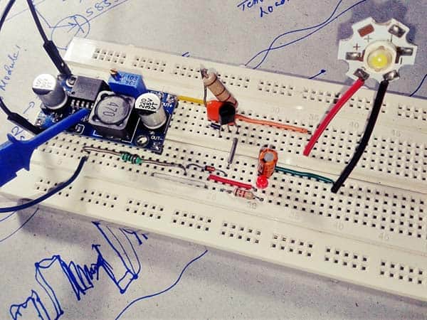
I wanted a variable load for testing small dc power supplies and tried many rheostats but they are beefy, clumsy and very expensive. So I decided to build a little variable dc load that would imitate a resistive load and that would also work as a portable device. After a bit of work, I came up with this astoundingly simple hardware solution. Here is the schematic of my simple electronic dc load, realized with a handful of inexpensive and easily available components.
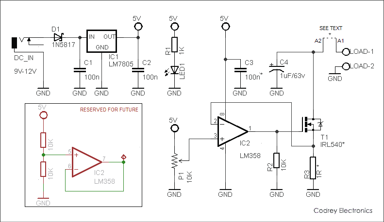
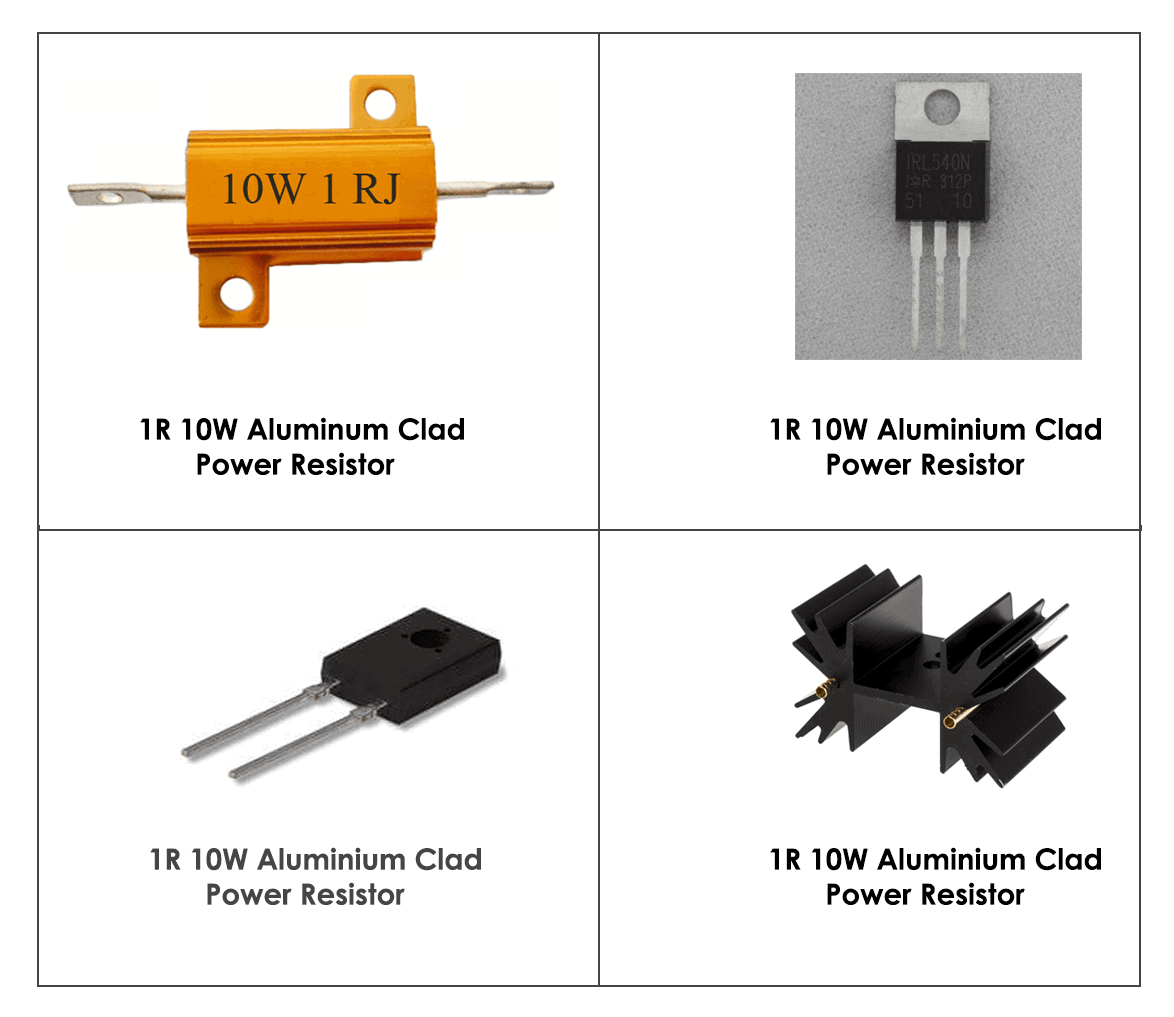
One-part of an LM358N op-amp (IC2) is used here as the core component. The 10K multi-turn preset potentiometer (P1) lets you adjust the current fine and precise. I have designed the circuit to use a logic level MOSFET IRL540N (T1) so that we can power the circuit from a voltage much smaller than 9V. Any logic level power MOSFET with an appropriate voltage/current rating should do, but I also tested the design with another MOSFET IRLZ44. Since the MOSFET works as a resistive element, it dissipates heat depending on the current flowing through it. To extend the power range of the load, you need to attach a suitable heatsink to the MOSFET. Similarly, the 1R resistor (R3) dissipates quite a bit of power, a proper heatsink is crucial here, too. The 1uF capacitor (C4) across the MOSFET is very essential to prevent unwanted oscillations.
The design theory is based on the voltage comparison of the inverting and the non-inverting inputs of the opamp, configured as a unity amplifier. When you set the voltage applied to the non-inverting input by adjusting the preset potentiometer, the opamp applies a certain voltage to the MOSFET gate. Depending on the gate voltage, the MOSFET will draw a certain amount of current until the voltage across at the current sense resistor is equal to the voltage at the non-inverting pin. In short, constant power mode is achieved here by calculating the desired set current via the measured load voltage.
Word of advice
The load input voltage is limited mainly by the drain to source voltage (Vds) rating of the MOSFET, and current by the value of current sense resistor. Take note, while connecting the source to the load, you should calculate the power dissipation carefully to retain the MOSFET always in the safe operating area (SOA) otherwise it will be deep-fried as soon as its die temperature exceeds the safety margin.
Regarding heatsink selection for the MOSFET, a standard TO-220 type with a thermal resistance of 2.50C/W should be a good pick. Since the typical junction-to-case thermal resistance of MOSFET IRL540 is 1.00C/W, case-to-sink thermal resistance is 0.50C/W, and maximum operating temperature range of 1750 C, the maximum power dissipation allowed will be 1750C – 25 0C (ambient temperature) / 40 C/W (total thermal resistance) around 37W. Similarly, try to use a 1R/10W-50W aluminum clad power resistor as the current sense resistor. If possible opt for the better TO-220 type power resistor (naturally with a heatsink) as it’s more convenient and efficient. Also, it’s good to attach a digital ammeter in series (see A1 & A2 in the schematic) to the load path, to measure the current drawn from the source.
Confession
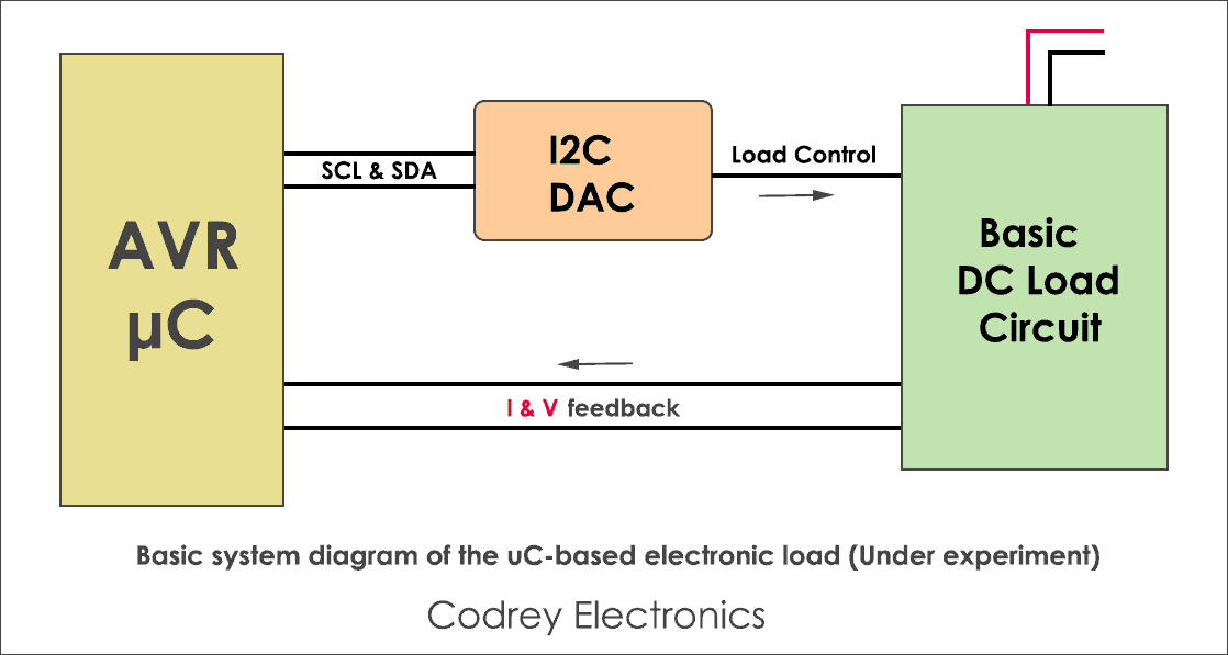
Because of limited resources, I rigged up my prototype without decent heatsinks. I built the circuit up on a breadboard and was only intended to be temporary till I make a PCB, but it really works well. My prototype was tested with a 5V/2A power supply. Decidedly there are improvements to be made, and one thing I would do if I do another revision of this design would be to add more features (probably by a microcontroller) to enhance reliability and safety. Anyway, this is a fun little project that I wanted to share!
Betterment’s
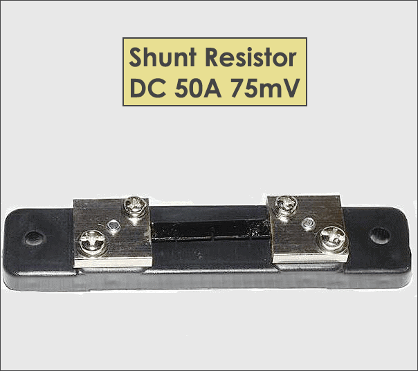
Since the IC has two opamps in it, you may as well put the other to use, for example, to build a test point for checking the load current. Also, the choice of an opamp is quite important here because what actually in demand is something can handle rail-to-rail voltages well, and have low offset voltage for accurate operation (the famed MCP6002 turns out to be a good pick as well). Similarly, there is a family of the so called linear MOSFETs specifically designed to operate in the linear region with an extended FBSOA (Forward Bias Safe Operating Area). So in the text book, they would be perfect for using in an electronic dummy load. Finally, if you modify your circuit extensively to sink very large currents, then it’s better to replace the current sense resistor with the very popular 50A/75mV (1.5mV/A) current shunt.
LM358 is not rail-to-rail, so feeding it the same 5v as the pot will make the output of the opamp to clamp at around 3.8v, Am I correct?
Shouldnt be powered from a higher voltage? for example the main DC-IN 9-12v?
Joe: Now I’m working on an advanced version of this design. Probably you can see that version here within a couple of weeks.
Regarding your query, yes you’re right! Common op-amps often need to have inputs a little less than positive rail and a little more than negative rail. For a unity gain follower with 0V input (with 12V vcc, the output swing lies in 100mV – 10 V range). A voltage follower/voltage buffer, – also known as a unity gain amplifier – has a gain of 1, So on paper the output voltage is equal to the input voltage. Of course, there are limits to the ability of the output to follow the input. As the input voltage swings positively, the output at some point near the positive rail will be unable to follow the input. Similarly the negative output swing will be limited to somewhere close to ground rail. In short, the output strictly follows the input as long as the input level is within the op-amp’s “usable” scale
When it comes to LM358 in particular, it’s not a rail-to-rail op-amp, hence its voltage levels will be throttled. Actually, LM358 allows its inputs to go down to the negative rail, but does not allow the inputs to get closer to the positive supply rail than 1.5V (i.e. 3.5V @ 5V VCC). Further, there’s a drop in the output voltage (usually 1.4V,).
Thanks for your feedback,, and keen interest!
Hi, I built this and works great. I tried to use the second op-amp to turn a LED on when the battery drops to 3 volts but can’t get it to work at the right voltage. I have the inverting input to a voltage divider set to 3v and the non inverting input to battery positive and 330 ohm resistor from +5v to Led to op-amp output. Do I need some decoupling ?
Kirk.
Kirk: Glad to see your feedback. Thanks!
Better, apply a zener diode-based fixed reference voltage to the non-inverting input, and then feed the battery voltage input preferably through a potential divider to the inverting input. Finally wire the LED between LM358’s output and GND rail through the current limiting resistor.
This is a basic reference https://2.bp.blogspot.com/-QRUsCvDCsMw/WJGsKuzDvmI/AAAAAAAAAkI/uspZoDmjKd0b8tzq4FWBG8TgQgsA5WfcQCLcB/s1600/12BatteryLevelMonitor.png
BTW, I’ll come up with an improved idea later. Stay tuned!
Thanks for the quick reply, I will give that a try.
Can I use IRZ44N MOSFET which is not a logic-level MOSFET?
Also, can I get to know more about why logic-level MOSFET is used in this application rather than just using a common non-logic level MOSFET?
Thank you.
It’s because logic level needs low voltage of 0v to 5v at the gate Vs not logic level mostfet needs about 10v at the gate if not it will not put anything like high current non logic level needs at last 6v at gate source but only problem is that it needs higher than 10v to get full current load
good evning,
have been looking for a DC load for testing all kinds of things,
will really read the description and comments closley. thanks for the insight. Dan, UK.
@dan: I understand that you are looking for a DC electronic load with advanced measurement features such as constant current (CC), constant resistance (CR), constant power (CP) etc.
I haven’t designed such a microcontroller based circuit yet but will try later. Thanks!