The power sequence is the sequence in which the power is applied and shut down between steps in a sequence. A power sequence is used when there are devices with different power supply voltages mixed together on one system, or when multiple equipment is connected. In this post, you can see the design idea of a simple do-it-yourself power sequencer which can be used to activate and/or deactivate AC or DC powered equipment on-site or in a remote location step-by-step. Sequencing can be initiated by an internal push-button switch or an optional external remote switch.
The Basic Circuit
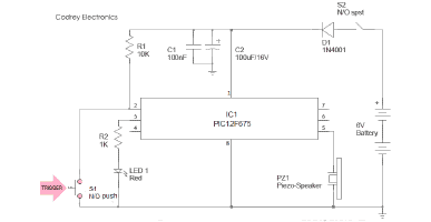
Well, let’s start with the basic circuit of the power sequencer. Not to mention, the basic design idea is very flexible and there is enough room for further expansion. As you can see in the below schematic, this part is centered around the evergreen CD4017B CMOS decade counter/divider IC (https://www.ti.com/lit/ds/symlink/cd4017b.pdf).
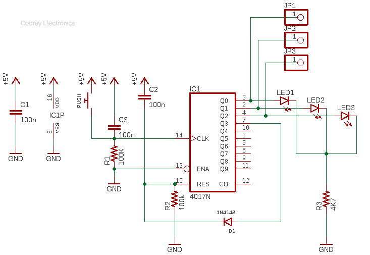
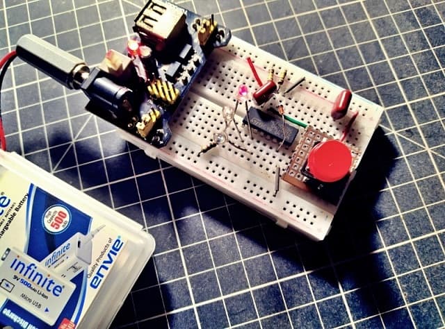
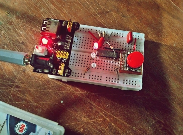
This circuit can be made using many different circuit construction techniques including stripboard, matrix board, breadboard, and printed circuit boards. This is a manual power sequencer, that means, the sequence is generated through a push-on button switch. Note that the circuit shown here has only 3 output channels with 3 indicator LEDs, but a more useful version would be made by linking electromechanical relays (EMRs) or solid-state relays (SSRs) with each channel (provide them all things required). In principle, up to 10 output channels can be set up for the power sequence because CD4017 has 1o decoded outputs (Q0-Q9).
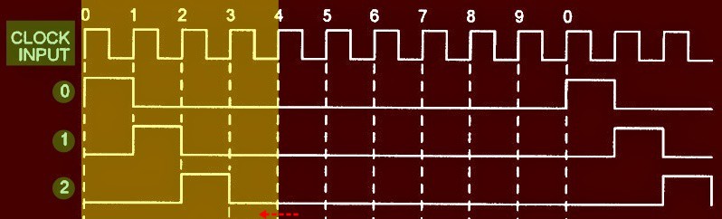
This is the timing diagram (Q0 to Q2 outputs) of the basic circuit presented above, with its “reset” and “clock enable” terminals (Pin 15 and Pin 13) grounded. The counters are advanced on the positive edge of the clock signal generated by the push button switch. The decoded outputs are normally in the logical “0” state (L) and go to the logical “1” state (H) only at their respective time slot. Each decoded output remains high for a full clock cycle.
An Elaboration
I certainly could have purchased a cheapo power sequencer, but then what fun would that be? Luckily, the heart of the power sequencer – CD4017B – offers a number of options to tweak the basic circuit idea. So, I am able to make it more useful with the help of a few more discrete components. Let me discuss the refinement thoughts one by one.
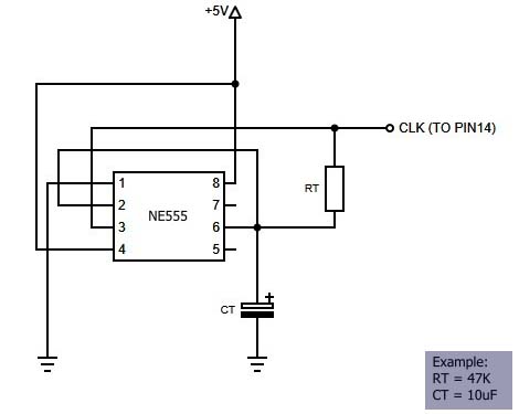
So, here’s a simple concept I modified to build an ‘automatic’ power sequencer. The underlying idea is to feed an adjustable low-frequency clock pulse to the clock input (Pin 14) of CD4017B IC. The circuit is fantastically simple to understand and easy to build.
At its simplest, you input a clock signal, and one of ten different outputs is set “High” while the others are all “Low”. On the next rising edge of the clock, the next output is on high and the previous is off. This goes on until the count loops around the end.
Back to what matters here. Now you’re going to make a clockable power sequencer circuit that’ll put out logic voltage signals on one pin after the other. The 555 IC can be wired as a clock pulse generator for this idea as shown below. Or you can use your own 555 IC-based astable oscillator circuit to do that. If so, see this page for 555 oscillator frequency calculations https://daycounter.com/Calculators/NE555-Calculator.phtml
Remember, the clock input needs to be a pulse. The counter is advanced when the clock signal rises from Low to High and there is no other timing involved. This means the clock signal can be as long or short as you like, but cannot be a single state change. Counting only advances on the rising edge of the clock signal i.e., a High clock signal has to go Low and then High again to step the counter.
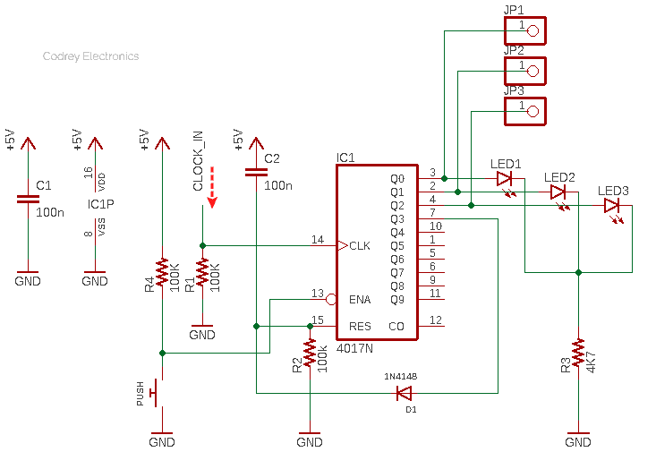
Now note that the push button switch in the basic schematic is intentionally moved to a new position. The push-button switch is wired to the clock enable (ENA) input (Pin 13) of CD4017 to taking it “Low” whenever the button is pressed and thus enabling the count to proceed. Enough of the talk. Let’s build!
The Load Driver Circuit
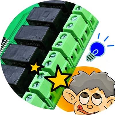
As you’re aware, a load driver is a circuit that has capabilities that allow it to be the electrically isolated interface between a low-voltage source circuit and perhaps a high-voltage load. An easy way to create the load driver would be to use an electromechanical relay. One challenge in using the CD4017 here is its limited output current source /sink capacity. So, we need suitable transistors to drive most available electromechanical relays.
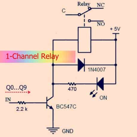
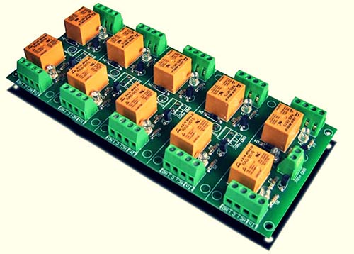
Below you can see a 10-Channel Relay Module available for cheap. This one is a general-purpose multichannel relay (power supply 5VDC) module for switching high-current electrical loads – both AC and DC. With this relay module, any dc input from 3V up to 30V can be used to activate a relay, and it may be controlled directly by a microcontroller as well. Luckily, this compact relay module can be used successfully with your CD4017B power sequencer prototype.
As an aside, if you look at the CD4017B datasheet, you can see that the current sink/source notations included there are a little weird. For example, I(OH) is -10 mA and I(OL) is 15 mA!
Don’t worry, just interpret it as you can “source” a load (connected between the output and GND) with 10 mA, and can “sink” a load (connected between VCC and the output) with 15 mA. See, when you are sourcing current, the current is extracted/subtracted from the output, therefore negative when you are sinking current, the current is added into the output, therefore positive!
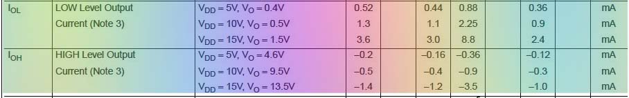
Also note that the datasheet just points out that at those current levels the output voltage will still meet the high/low logic voltage levels – it does not mean the output will set off at those values. You can source/sink more current from the output, if you don’t care about the voltage levels. But look at the absolute maximum ratings, and it’s certainly not a good design practice!
Revision Time
At this time, recall that the output of CD4017B changes sequentially from Q0 to Q9 for every high pulse at Pin 14, but this sequence can be interrupted by two pins – Pin 13 and Pin 15 – held “Low” by default. In the basic circuit (first schematic) demoed, when the count is at pin Q3, Pin 15 goes high, and the count will reset itself back to Q0 and will stay there until Q0 is made low again by the next clock pulse input. Similarly, if the count is at pin Qx when Pin 13 is made high, then the count will pause at pin Qx irrespective of the clock pulse input and will continue incrementing only when Pin 13 is made low again. Reading the CD4017B datasheet well will give you more confidence. So, spend some time on it.
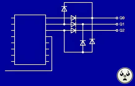
Moreover, sometimes you don’t need just momentary ON and OFF (L→H→L) outputs, but you need steady ON outputs (L→H) in succession. Also, here the basic theme comes in handy. You can try adding something similar like the “Micky Mouse Logic” (MML) to the basic circuit to fulfil that task (https://en.wikipedia.org/wiki/Diode_logic).
Closing Note
This very simple pulse sequencer concept offers an enormous range of application possibilities, and many variants of the basic design are possible. Not to mention, many methods for power sequencing exist, but in this project, I just looked at an entry-level power sequencer that is ideal for both small and large voltage and current switching.
I am still working on an extension of this project idea. After a short break, the project will get a new look and you can see it here. So, stay tuned for updates!