Let me have my say – it’s my habit to do things over again. Not a mere repeat of anything that fitted well, but wishing to try potential betterments at slightly different angles. Confused? Sorry, it’s off to a good start (once again) with the revered eight-legged timer chip – the 555!
In reality, the tiny timer chip hardly needs an introduction as we can see countless circuits revolved around this world’s best-selling integrated circuit since it was designed in 1970 by analog wizard Hans Camenzind. This article is just to help you play some tricks, in particular with the Pin 5 of 555 IC.
Pin 5 of 555, eh?
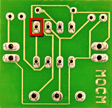
In most 555 circuits you can see that its pin 5 is hanging i.e. left unconnected or often ac coupled to ground rail through a 10nF capacitor. Next is the image of a 555 astable kit’s PCB. Catch the “free” solder pad for pin5 of 555.
Actually pin 5 is very useful as it’s the “Control Voltage (CV)” terminal (internally set to 2/3 the supply voltage) lets you control the threshold voltage (pin 6). In short, this enables you to vary the length of the output pulse in monostable mode and/or the output frequency in astable mode. Refer to the functional diagram:
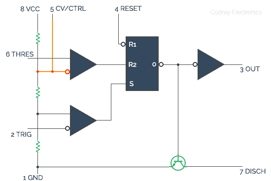
As you noticed, pin 5 controls the timing by overriding the 2/3VCC level of the voltage divider. So, output pulse width can be changed independently by feeding an appropriate voltage to pin 5.
Pin 5 Hack – Basic Idea
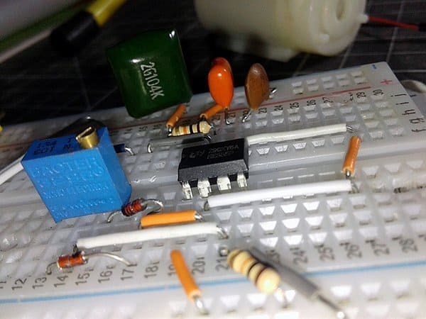
The 555 chip is extremely useful for building electronic circuits from simple timers to versatile voltage controlled oscillators. To explain the pin 5 hack I will start with one of the basic ideas. The circuit shown below lets you control the duty cycle of an inputted PWM signal within certain limits. For the purpose, a variable potential divider network is wired to pin 5 of 555, thus you can adjust the potentiometer in the network for varying the PWM duty cycle.
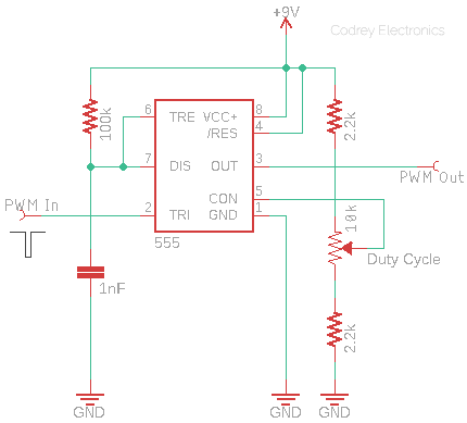
Wiper of the potentiometer (thus pin 5 of 555) sees a (theoretic) voltage near to 1.3V below VCC to 1.3V above GND. Actually, in monostable mode, the control voltage may vary from 45% to 90% of the VCC. Although voltages outside the limits can be safely applied, reliable operation is not warranted. The quick experiment was conducted with ~5kHz (99%) PWM signal (186uS mark /1.86uS space) as the input of the circuit, and attained sensible control over the duty cycle as calculated.
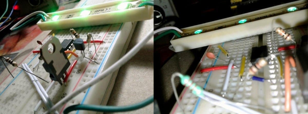
LED Driver?
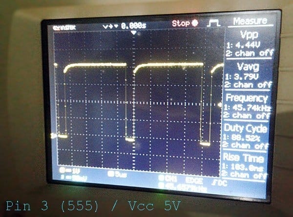
Since we can gain access to the 2/3 of the VCC on the internal voltage divider (upper comparator’s reference point) of 555 through pin 5, it’s easy to build a simplest LED driver by exploiting that opportunity. Take a look at the following experimental design and give it a try. 555 IC is configured here in astable mode for default Fosc around 47kHz (90%). Refer the scope trace included at the bottom of this article.
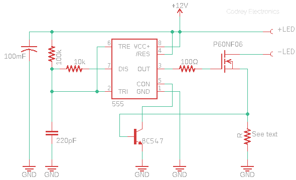
To set off the experiment, connect a 12V-type LED (like the 5050-3LED green sign module) and use one 2.2Ω resistor as the resistor R. Side by side, observe the duty cycle at pin 3 of 555 IC with 2.2Ω as R at first, and later with 10 Ω – 22Ω as R. Any noticeable change in the duty cycle, also in the brightness of the LED? Repeat the test with different known light emitting diodes and resistors to get a spark of interest!
As we have seen, feeding a control voltage to pin 5 will change the duty cycle and period (by variable high time and constant low time) of the output signal. The change is fundamentally linear if Vctrl < 2/3Vcc, so keep an eye on this while you’re setting your circuit up. If you’re in deep trouble, you will need to post your circuit here for further assistance.