Here’s a simple and clever way to build a toggle switch with a quite popular, highly available, and cheap CMOS logic chip CD4049UB. Since the little electronic toggle switch presented here is an easy to assemble one that approaches the performance of a mechanical toggle switch, just try it!
The heart and soul of the design
The basis for the toggle switch is CD4049UB hex inverting buffer and converter IC. This is a CMOS logic chip that contains six inverting hex buffers, and the attending electronics to make them work. The CD4049UB have standardized symmetrical output characteristics and a wide operating voltage from 3V to 18V. According to datasheets, CD4049UB is the industry’s highest logic inverter operating at 18V under recommended conditions!
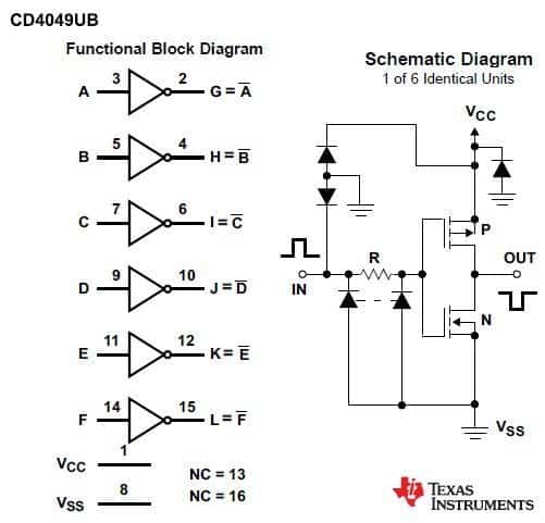
Somebody mighty wonder whether this is the correct thing to do, because there’s a pretty cool dual-D flip-flop – the CD4013 chip. Admitted, but there’re many other ways to do that, so I searched everywhere for an ‘unorthodox’ idea for my design, and eventually got an ingenious thought through an informative blog post published by R.G. Keen (http://www.geofex.com). Below you can see the tried and tested circuit diagram of my CMOS toggle switch with CD4049UB, based on that idea.
Circuit diagram and design description
The circuit diagram is extremely simple and self-explanatory to some extent. The circuit will be a great alternative for traditional simple toggle switch circuits and also proves to be more cost effective and reliable among many other design solutions.
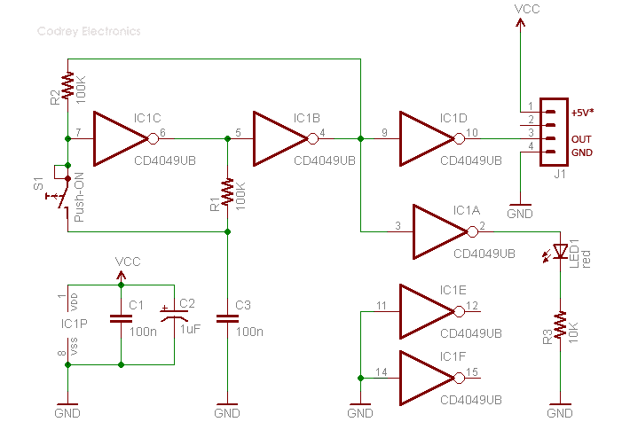
Even though the CD4049UB (IC1) can be powered from 3V-18VDC, a well-regulated (and clean) 5VDC power supply operation is recommended for the given design. Anyway you can power it up with dc voltages up to 9V without changing anything in the circuitry!
VCC terminal (pin 1) of IC1 must have a good bypass capacitor to prevent power disturbance, and a 100nF capacitor (C1) is wired there as recommended in the official datasheet. The 1uF parallel bypass capacitor (C2) is added deliberately to reject different frequencies of noise. The unused inputs of IC1 (Pin 11 & 14) are connected to the ground (0V) rail to prevent them from floating (you could always follow this rule).
Now to the working principle of the toggle switch circuit! Here, two inverters (IC1C & IC1B) form a latch. Assume that pin 6 of IC1 comes up high (pin 4 will be then low). The 100nF capacitor (C3) charges to +5V through the 100K resistor (R1) and stays there forever. However, if you push the momentary push button switch (S1) that bridges C3 to pin 7, the +5V on C3 pulls pin 7 high. The second 100K resistor (R2) prevents the low level output at pin 4 from driving back C3, so pin 7 goes high. That impels pins 5 and 6 low, which makes pin 4 high (Pin 4 makes pin 7 high as well). With a second trigger by S1, the flip will be flopped!
Next gate (IC1A) is used to drive a low-current indicator (LED1) that wakes up when the toggle switch is in its ‘on’ position. When toggle switch is in its ‘on’ state, another gate (IC1D) will deliver a logic-high level output through its output terminal (pin 2). From there you can take the ‘buffered’ logic-level output to control/switch an external circuit or device as desired.
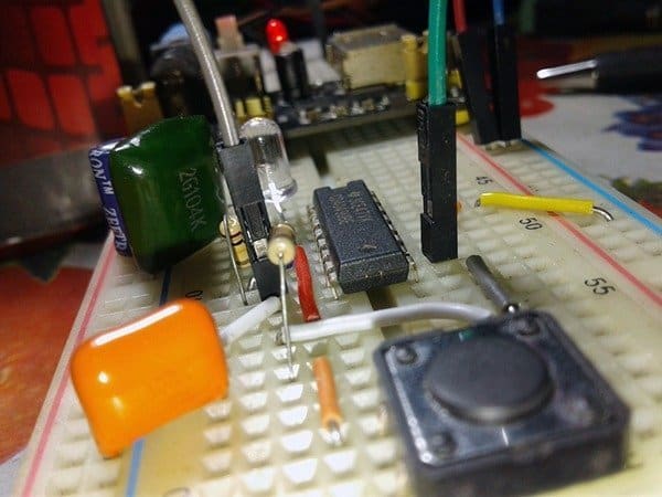
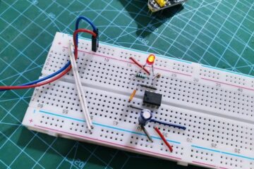
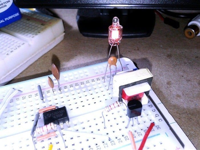
This is my quick 5VDC powered breadboard setup. But you should build your circuit on a piece of small veroboard by soldering all components while keeping the interconnections as short as possible. Although this is a very basic and simple to construct electronic toggle switch circuit, it’s guaranteed to lock up the final output either fully logic-high, or fully logic-low as explained!
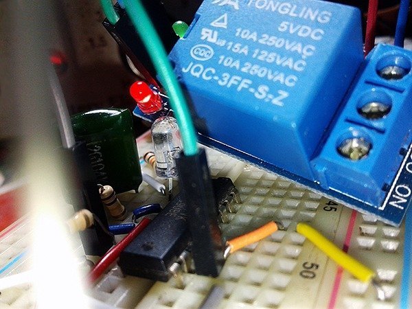
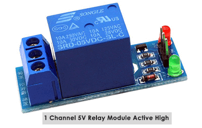
The most preferred and easy method to control a CMOS logic chip is with another one. So you can exploit the logic-level output(s) of this toggle switch circuit to drive another CMOS chip in a circuit, to say, a ‘quad bilateral switch’ like the CD4066 used mainly in an audio electronics. However, if your real intention is to switch an electric load on and off, then simply add a suitable electromagnetic relay (or a solid state relay) at the output of the toggle switch circuit for that task (ofcourse with its driver electronics). The quick way then is the use of a pre-wired “1-channel 5V relay module (active high)” similar to the one shown below. Since you have two more ‘spare’ inverters in the toggle switch circuit, you might as well use them for controlling/driving different relay driver modules or the like.
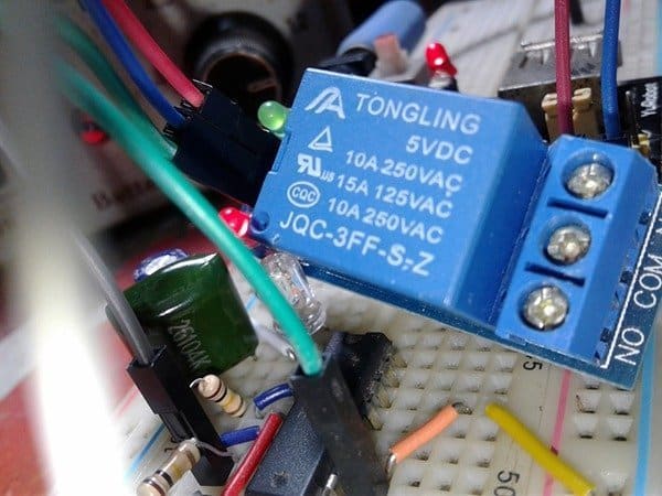
Following is a casual snap of my play with a 5V relay module, I bought from online for cheap.
And for serious makers, a simple transistor based relay driver circuit can be used in place of the Chinese relay module.
Get creative, and see what happens!
A revision has its own peculiar pleasures and its own peculiar frustrations. Anyway, I am happy with the results that I’ve obtained, and perfectly proud of the experiment I did, looking back at it. Finally, I’d love to hear what you think I should tackle next…
Cool! I like this. Can I bum a favour? Could you tell me the values if I power this from 12 Volts? Cheers!
Andreas Hierzenberger: Thank You! As you may know, you can employ a cheaper 5V regulator module to power this circuit from the 12V DC input instead of extensively modifying the entire design. See https://www.ebay.com/itm/5V-Regulator-Module-1117-Voltage-Regulator-Power-Supply-Module-800mA-for-Arduino-/222482868369
I’d like to try your layout, thank you for your work.
Glad to note. Thanks!
Soon I will add some interesting stuff here. Enjoy!