Of late I asked to control certain devices through a MOSFET from an Arduino microcontroller, but the devices are 12VDC rated and demand much more current than the Arduino can deliver. The easiest way to do that is with a logic-level MOSFET but my client did not want to go for that, as the intent is to use a cheap standard MOSFET and to turn it fully on with most modest power loss.
Design Requirements
- Input must be governable from 5V and 3.3V microcontrollers
- Must be able to handle a couple of Amperes
- Must be a Power MOSFET based driver circuit
- Must work with 12VDC
Output must turn on during power on or if unconnected
Design Schematic
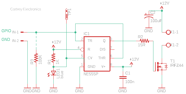
Aware that a standard Power MOSFET requires a gate voltage higher than an Arduino I/O can render and hence a driver circuitry is required in-between. At first, I prepared a quick setup with a MOSFET gate driver chip TC4427 to ‘fire’ one IRFZ44 Power MOSFET because I’ve ready access to a 12VDC source for driving the gate.
Sadly, my client denied my quick scheme centered on the pricey TC4427 gate driver chip!
So, I reformed the concept and tailored a digital MOSFET switch module, a cheap and cheerful circuit based on the ubiquitous 555 timer IC. It’s fairly a simple design, 555 timer chip as a standard MOSFET driver to do the level translation from 5V to 12V.
Admitted, you could also use a regular BJT to construct a driver circuit and then use it to control the power MOSFET if a 10V- 15V source for driving the gate is available. But my intent was to put up a new idea!
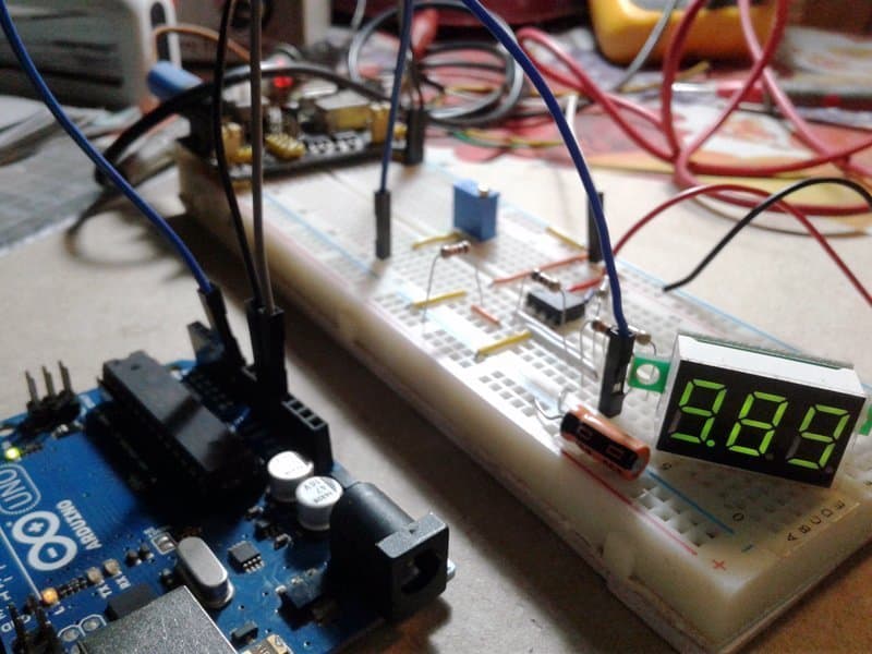
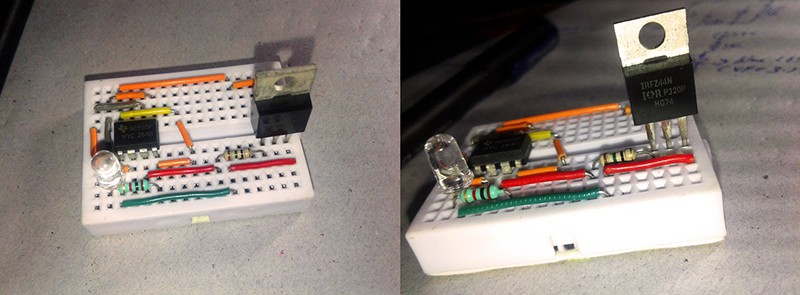
This is my mini breadboard setup of the entire design. Note that the breadboard assembly missed capacitors C1 and C2.
Design Insights
The design is basically a 555 inverting buffer (Schmitt Trigger). Since it’s an inverting buffer, the output logic state (L/H) is the inverse of the input state (H/L):
- Input low (< 1/3 Vcc) makes output high
- Input high (> 2/3 Vcc) makes the output low
When the input voltage is between 1/3 and 2/3 Vcc, the output remains in its current state. This intermediate input region is a dead space where there is no response, a property called hysteresis. The trigger input (pin 2) and the threshold input (pin 6) pins of IC1 are tied together, and with a 12VDC supply, the upper threshold is 8V (2/3 Vcc) and the lower is 4V (1/3 Vcc). These two voltage levels, being far apart, make a great Schmitt trigger, which may be driven directly by a CMOS logic that is also powered by 12VDC.
However, to make it harmonic with TTL (5V) logic levels, a slight modification of IC1’s control input (Pin 5) is essential. The tricky combination of one 1K resistor (R1) and a basic 5mm blue LED (VF=3.1V) loads down the internal divider of 555 IC to a lower voltage. You may replace the LED circuitry with a potential divider (3.3K upper resistor and 1K lower resistor) so that TP1 can see a fixed voltage there – the estimated levels are about 1.4V and 3.0V respectively!
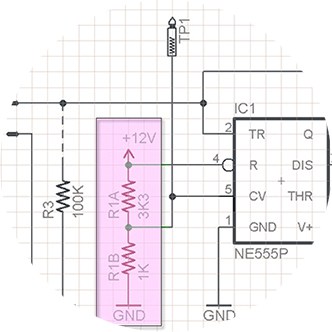
The operation of this circuit is simple. The circuit toggles T1 when input is available – when the input (Pins 2&6) of IC1 is low its output (Pin 3) is high and T1 conducts to fire the 12V load wired to connector X1. When the input is high, the output becomes low and T1 is released. The 100K pull-down resistor (R3) is an optional component. Note that when you connect power to the circuit T1 is engaged.
The IRFZ44 (T1) is a 60V [VDS (V)], 50A [TC = 25°C, VGS at 10V] TO-220AB Power Mosfet preferred for commercial-industrial applications at power dissipation levels to approximately 50 W. Its RDS(on) is 0.028 Ω at 10V VGS..
Pin 6 (Threshold) of 555 IC is the non-inverting input for comparator #1. When the threshold voltage is greater than 2/3 Vcc, the output of the comparator #1 goes high which resets the flip-flop and turns the output off (0V). Likewise, a voltage less than 1/3 of Vcc on pin 2 (Trigger) triggers the internal flip-flop via comparator #2, and pin 3 (Output) switches from low (close to GND) to high (close to Vcc).
However, the requisite 2/3 Vcc level (8V incase of 12V Vcc) is not available from the GPIO of a 5V microcontroller. Therefore a tricky setup (R1+LED1) is employed there to override the default threshold values. See, the control pin (Pin 5) is used to control the trigger and threshold levels, and these levels can be modified by applying a voltage to the control pin, either from an active circuit or by connecting a passive potential divider between Vcc and GND.
Construction & Test
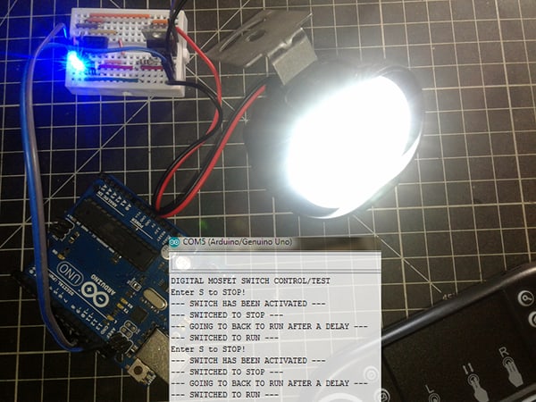
The whole circuit can be constructed on a piece of the common perforated circuit board. Since all parts are ‘leaded’, soldering and assembling will not be too difficult. After assembling the board, it’s time to test the prototype with the small Arduino sketch (actually the snippet of a big code) given below.
int drivePin = 13; // Pin number for the drive pin
int switchDelay = 6000; // Pause to provide a transition delay


void setup() {
  pinMode(drivePin, OUTPUT); // Set the drive signal pin as an output
  digitalWrite(drivePin, LOW); // Set the drive signal to off by default


  Serial.begin(9600); // Launch the serial monitor
  Serial.println("DIGITAL MOSFET SWITCH CONTROL/TEST");
  Serial.println("Enter S to STOP!");
}

void loop() {

  if (Serial.available() > 0) { // Check if data is available on the serial input
    char input = Serial.read(); // Store the serial data in a variable
    if (input == 'S') { // check if the incoming data is the letter 'S'
      Serial.println("--- SWITCH HAS BEEN ACTIVATED ---");
      Serial.println("--- SWITCHED TO STOP ---");
      digitalWrite(drivePin, HIGH); // Set the switch to STOP
      Serial.println("--- GOING TO BACK TO RUN AFTER A DELAY ---");
      delay(switchDelay);
      digitalWrite(drivePin, LOW); // Set the switch to RUN
      Serial.println("--- SWITCHED TO RUN ---");
      Serial.println("Enter S to STOP!"); // Resend the instruction

    }

  }
}
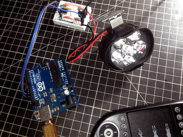
If you have never tried programming an Arduino with the Arduino IDE, more on this subject can be found elsewhere in this website and many other websites, as well as in tutorials. The next figure gives an impression of the rude test setup – for the agile test I have used my breadboard setup which with a bit of luck can be used for a few days of evaluation. Yes, there’s still some serious work ahead of me – the first one is the design of a stunning PCB.
In the above code, D13 of Arduino Uno is configured as the drive signal output pin. Here, the Power Mosfet Module can be toggled by keyboard input, that is simply a character ‘S’.
A side note: I think I made a minor mistake! According to the datasheet, the input capacitance of the IRFZ44 is typically 1900 pF. Since the bipolar 555 timer chip is rated for 200mA sink and source current, it’d better use a 100Ω resistor in place of the 15Ω gate resistor (R2) used here to ensure that the current would always be below 120mA.