What is the point in critiquing a cheap Chinese power MOSFET module, you might ask. But I have a reason for that, because learning something useful from other people’s mistakes (even if they are trivial) is a good habit we should follow.
So, in this post you can find my notes and thoughts on an easily available and cheap dual power mosfet switch module. OK, let us get started…
A quick look at its key features
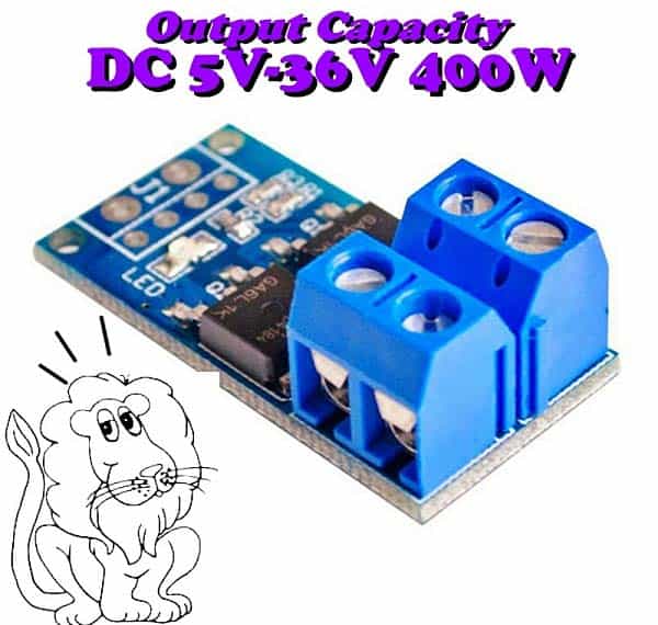
As reported by the online seller, this is a 15A/400W dual power MOSFET module that has the following features:
- Output Drive Capacity: DC 5-36V
- Output Current: 15A continuous, 30A burst
- Output Power: 400W max.
- Trigger Source: Digital High/Low (DC3.3V-20V)
- PWM signal Frequency: 0-20kHz supported
- Operating Temperature: -40-85°C
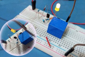
The module employs two parallel-connected N-Channel logic-compatible power MOSFETs for high-current low-side switching applications. Needless to say, this module expects two connections – an input signal to turn the MOSFETs on/off and a DC power supply to power the load being controlled. While it may seem a bit complex, just follow the wiring diagram shown below.
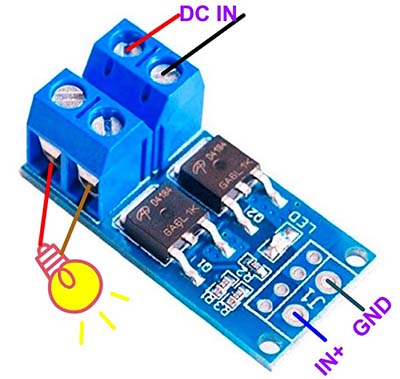
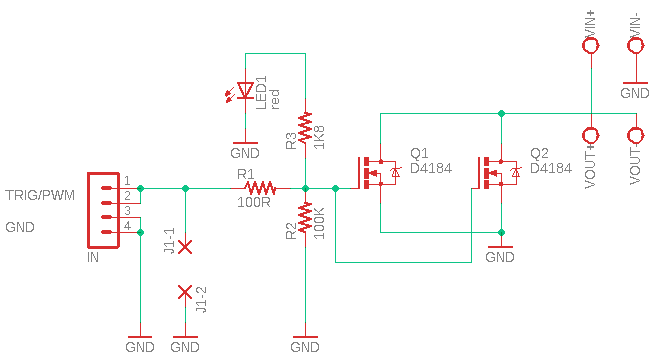
This is the rear view of the module. Its PCB power tracks, as advertised, can carry high currents for mighty loads. As you can see, this module has two D4184 power MOSFETs (http://www.aosmd.com/pdfs/datasheet/AOD4184A.pdf). Below is the basic schematic of the module (drawn by me).
A quick look at its design flaws
How good is the design of this module? Are there any hidden downsides?
Yes, I feel some flaws in this design. The first and most obvious mistake is in the parallel configuration of the power MOSFETs. So, how bad is it? Well, let us see!
Like any other component (linear or nonlinear) power MOSFETs can be wired in parallel. The advantages of hooking up MOSFETs in this way is that the total current is split evenly among each MOSFET (assuming they have the same on-state resistance) which then scales down the amount of heat they generate.
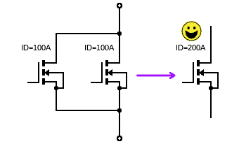
So, from a theoretical standpoint, MOSFETs put in parallel can be treated as a single component, and it is a common practice to use the parallel configuration since it results in an effective diminution in RDS(on) that can still be handled by a single gate driver.
However, it is well-advised that each MOSFET in such a combination should have an individual gate resistor (resistor placed between the gate and the shared connection to the gate driver).
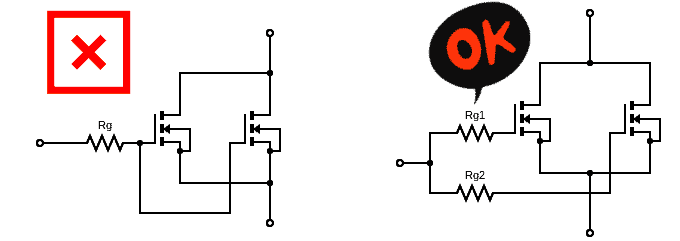
This is because, when the first MOSFET turns on, it causes a rapid voltage swing at the source point as it starts to conduct, then span through the parasitic gate-drain capacitance of the next MOSFET, and cause a voltage spike on the shared gate connection. This results in oscillation on the gate point as the MOSFETs rapidly turn on and off, and eventually destroy the gate driver or MOSFETs. But individual per gate resistors can dampen this effectively. Sadly, this dual MOSFET module has no individual gate resistors.
Moving on to the next flaw, while the module is technically 3.3V logic compatible, the D4184 MOSFET has a Static Drain-Source On-Resistance/RDS(on) of 9.5mΩ maximum (at 4.5V VGS). Since the module puts two of them in parallel, this will be halved to about 4.8mΩ maximum but the load current may then need to be kept down marginally (<10A) to avoid overheating of the mosfets, especially when using a gate drive signal under 4.5V (the mosfet achieves its minimum on state resistance at 10V VGS and therefore has the most modest possible power dissipation).
Next important point to take note of is that this module does not have a flyback diode onboard. So, when an inductive load is being operated, an external flyback diode should be used.
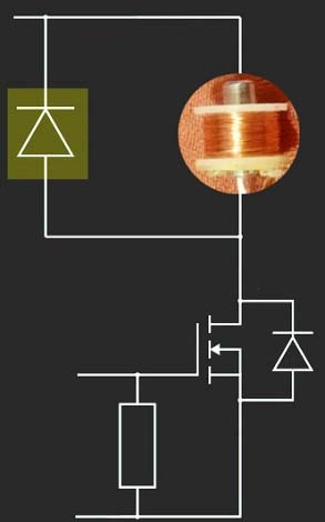
The purpose of the flyback diode is to protect the MOSFET from an inductive flyback otherwise it will sooner or later destroy the MOSFET. Inductive flyback (also known as inductive spike, inductive kickback, back-emf, etc) refers to the phenomenon of a large voltage spike that occurs when the power to an inductor turns off and the magnetic field around it collapses (https://en.wikipedia.org/wiki/Flyback_diode).
Jumping to a quick conclusion
A (not so) shocking revelation is that most Chinese manufacturers are able to make modules with virtually no critical parts (ha ha).
The module does not deliver what it promised on the description (at least in my view). Anyway, you can expect about 2/3 of the stated capacity to be really available. That being said, the module is actually usable if you take the stated capacity with a pinch of salt and you do not mind that the module does not perform well together with certain pulse width modulated signals.
Well, I am not going to test the power handling capacity of this module with a TTL/CMOS on/off or PWM signal input at this time. In an upcoming practical project, I will explore more. So, watch this space for cheering updates!
Dear T.K. Hareendran . I understand fully the problem with the two resistors. So I want to design a new PCB for myself with the two resistors. Is it correct to put the 100 Ohm resistor beyond the nut where the other two resistors are placed and then use for every mosfet, and the must be 100 Ohm? Thank you in advance!
@Marcel: Hopefully the hints in this document (https://www.ti.com/lit/an/slvaf39a/slvaf39a.pdf) will help you design and build a dual-MOSFET module.
Thank you for reaching out and expressing keen interest in my article. Cheers!
Hello,
Thank you for the article. I recently received some of these. I was disappointed for a couple of reasons. First, I saw two mosfets and assumed incorrectly they were connected as an a.c. switch. Second is a reason that might be worth noting.
The design follows Asian standards and use a positive ground where western design uses a negative ground.
With regard to the suggested second gate resistor, the board can easily be retrofitted with that component.
Thanks again for the article. I asked the seller for a schematic but got a photo of the pcb bottom. I was making my own schematic when I ran across yours with google.
Jim Julian
Jim Julian: Welcome, and thank you for sharing your thoughts!
Certainly these are general-purpose (or hobby-level) cheap Chinese dual-Mosfet modules. Well, now I have the design idea of a high-side Mosfet module that can safely cater ample high currents for resistive, inductive, and capacitive grounded loads according to stringent automotive demands. The idea will be posted here after a few weeks. See you then. Cheers…