After seeing an old LM324 chip-based thermostat kit in my attic, I decided it was time to whip up a quick refresher on the far-famed LM324 quad operational amplifier IC. I hope it can be practicable to someone here!
LM324 – Brief Overview
The LM324 IC consists of four independent, high gain, internally frequency compensated operational amplifiers in a single package which was designed specifically to operate from a single power supply over a wide range of voltages (operation from a split power supply is also possible).
Recommended operating conditions taken from a TI datasheet are listed below.
- Minimum Supply Voltage (V+MIN) : 3V
- Maximum Supply Voltage (V+MAX): 32V
- Minimum Operating Input Voltage (on input pins): 0V
- Maximum Operating Input Voltage (on input pins): V+
- Operating Junction Temperature (TJ): 0 to 70°C
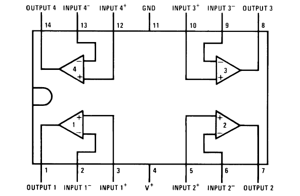
Following is the connection diagram from the same datasheet.
…and the schematic diagram.
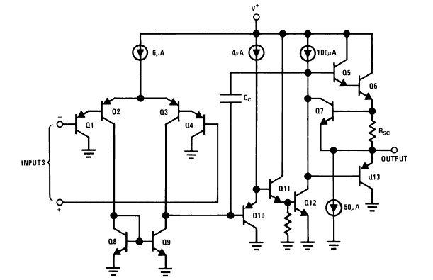
Note that LM324 is not a rail-to-rail operational amplifier, so the maximum output voltage is roughly 1.5V to 2V below VCC. Likewise, the minimum output voltage is around 5mV to 20mV above VEE/GND. The typical source output current is -30mA and the typical sink output current is 20mA.
LM324 – Quick Practice
Practice makes perfect, so now let us make a simple LM324 IC-based circuit using a handful of components lying around.
The proposed build is a single op-amp triangle wave generator. Here the single operational amplifier setup uses positive feedback with hysteresis to create a square wave, which charges and discharges an R-C network, which roughly generates a triangle wave.
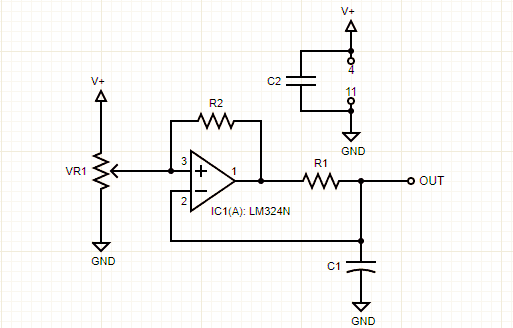
The frequency is determined by the R1-C1 integrator while variable resistor VR1 is used to control the symmetry of the triangle wave (it should be set at or near the middle scale of the wiper).
Note that R2 is there to add hysteresis to make the triangle wave possible, so the amplitude of the wave, in reality, depends on VR1, R2, V+, and the maximum output voltage swing of the op-amp IC1(A).
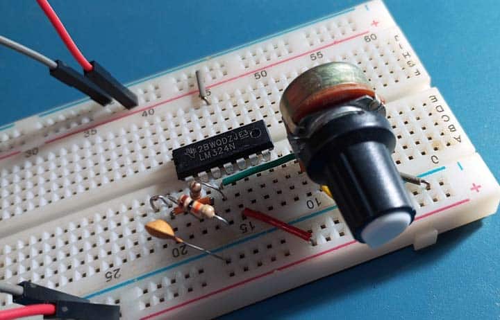
Below is an example list of components from a recent attempt I made.
- IC1: LM324N
- VR1: 50KΩ
- R1: 10KΩ
- R2: 470KΩ
- C1: 100nF
- C2: 100nF
- V+: 9VDC
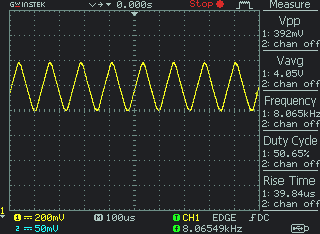
And, the observed outcomes…
- Frequency: ~8kHz
- Output VPP: ~400mV
- Output VAVG: ~4V
If you want to remove DC bias from the final output (OUT), then you will need to add a suitable coupling capacitor on the output.
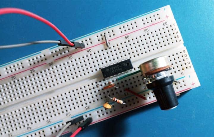
Here is my test circuit – just a quick breadboard setup:
In Conclusion
Frankly, there are a couple of drawbacks to this simple-to-experiment and implement concept – but that is only half the story!
Another practicable solution is to use a spare operational amplifier as an active integrator instead of the passive integrator setup in the given circuit configuration.
Then the two op-amp design generates a square wave and integrates it to make a triangle wave. In my view, this is overall less dependent on component tolerances and operational amplifier specifications and hence more consistent.
I will post about more of the examples over the next few weeks. Well, see you then!