There are certain applications that require only very low current and loose output voltage regulation. For such applications, a linear regulator made of discrete components is a quick and easy solution.
For those who want to “do it differently” and are looking for a unique but simple discrete linear voltage regulator design that does not use any special ICs, this post has some practical tips to help with that. As there is no better way to get a line about something than to learn by doing it, this would be a great idea for a good start…
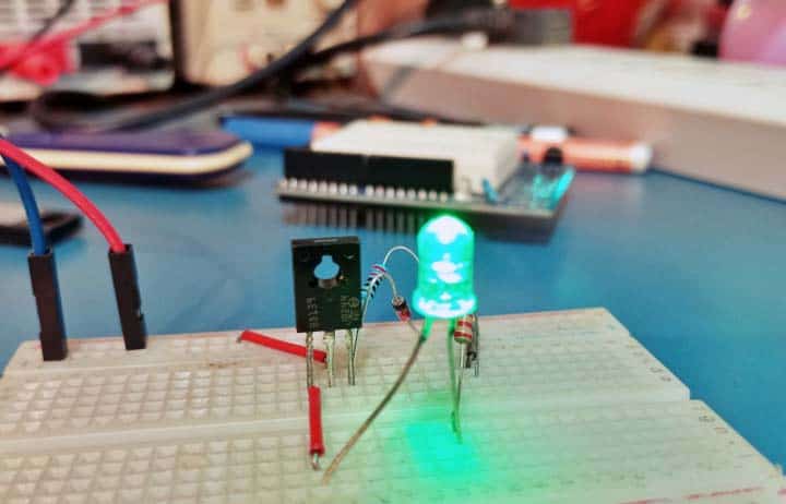
The drawing below shows a simple discrete linear voltage regulator. This is a very common basic design broadly used before the advent of 3-terminal fixed voltage regulator ICs.
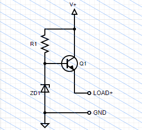
Here, the resistor R1 and zener diode ZD1 form a simple shunt regulator. If the voltage across the zener diode tries to exceed its breakdown voltage, it will conduct as much current as is necessary to keep the voltage at that level. And this keeps the base of the emitter-follower transistor Q1 at a constant voltage.
The NPN BJT (Q1) is the most crucial component. While selecting it, ensure that it should meet the following requirements:
- Its collector-to-emitter (VCE) and base-to-emitter (VBE) breakdown voltage should be higher than the maximum input voltage
- The maximum permissible collector current (IC) should be greater than the maximum load current (IL)
The output voltage is the reverse zener voltage (VZ) subtracting the transistor base-to-emitter voltage (VBE). So, choose the zener voltage 0.6V higher than the desired output voltage.
The base pull-up resistor R1 provides current for both the transistor base and zener diode.
The zener diode reverse current (IZ) should be greater than 1mA. In practice, it would be better to run the zener diode between 10-50% of its maximum power rating.
As an example, in case of a 5.1V/500mW zener diode, the maximum current that can flow through it is 500mW/5.1V= 98mA. So, 10-50% of that current is 9.8mA-49mA.
Next, this equation estimates the maximum base current required for operation:
IB_MAX = IO_MAX/hFE_MIN
As an example, the BD139 transistor has a minimum hFE around 50 at 150mA IC.
So, for rendering 150mA output current, IB_MAX = 150/50 = 3mA.
We need to add this 3mA maximum base current to the 9.8mA minimum zener diode current to work out the minimum total current required (3mA+9.8mA=12.8mA).
Well, let me now do a rough homework for my discrete linear voltage regulator design…
- Minimum Input Supply = 9V
- Maximum Input Supply = 12V
- Regulated Output Required = 4.5V
- Maximum Output Current Required = 150mA
- BJT = BD139
- Zener Diode = 5.1V/500mW
R1 maximum value: 9V-5.1V/12.8mA = 305Ω
R1 minimum value: 12V-5.1V/49mA = 141Ω
Thus I will start with a 220Ω resistor as R1 since it fits nicely between the minimum and maximum resistance values.
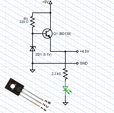
On this point note that ‘R1 maximum’ is the maximum resistor value to get rich current when the input supply is at 9V. Likewise, ‘R1 minimum’ is the minimum value to prevent potential excessive current flow when the input supply is at 12V (if you find any factual mistakes in my calculations, simply drop a comment below).
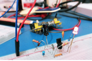
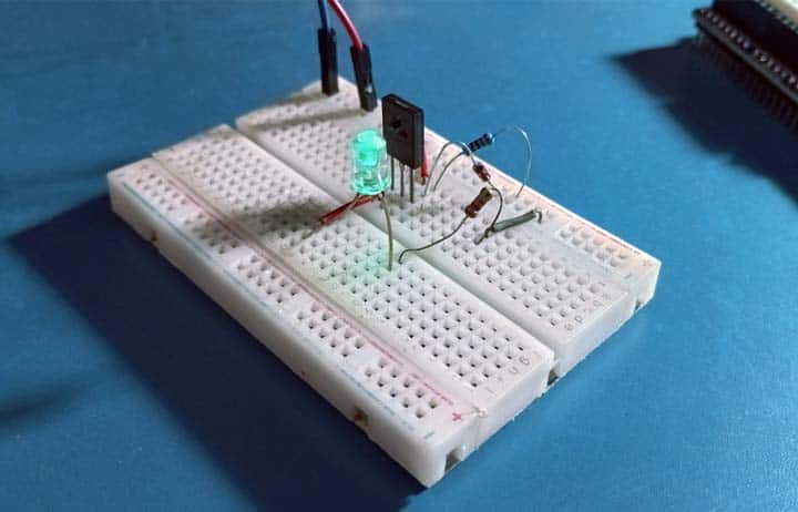
Ok now let us see the breadboard version I made for some quick tests.
It is obvious that this basic circuit can have surprisingly good performance with a few additional parts.
As an example, using a capacitor across the zener diode helps improve ripple filtering, and an appropriate heatsink keeps the transistor cool in toughest operating conditions. Also, putting a resistor across the output will constantly draw a feeble current, thus avoiding the slight increase in the no-load output voltage.
Finally, I will not go into an in-depth design analysis or component stress analysis now, but I am sure you can do it well. Keep Experimenting…