This article shows you how to use reverse voltage protection with minimal power loss in your electronics projects running on a battery/DC power supply. In fact, for a long time, I wanted to put together some reverse polarity voltage protection design ideas in a single post. As its outcome, here you can see a summary of my random thoughts. And, as a bonus, a self-do project is included at the end for you. Okay, get ready to grasp a few simple ideas you can use to help prevent that magical smoke from getting out of your priceless prototypes!
The Series Diode Trick
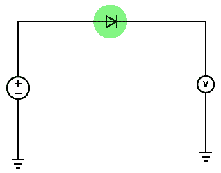
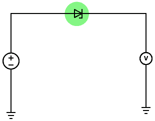
The simplest protection against reverse voltage protection is a diode in series with the power source, as seen in the below figure. Here, the diode becomes forward biased and the load’s normal operating current flows through the diode. However, if the power source is connected backwards, the diode reverse–biased and no current flows!
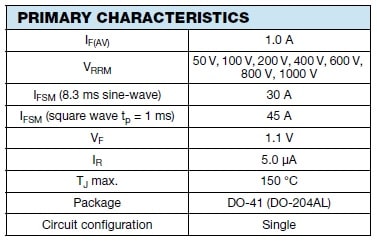
You can simply use a regular general-purpose plastic rectifier like the 1N4007 for this trick. The 1N400x series diode will handle load currents up to 1A and a 1N540x series will work up to 3A, but note that the diode will drop about 0.6 to 1.1V (VF). The wasted power then will be VF x I.
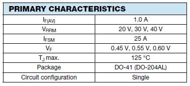
To minimize the above-pointed disadvantage, you can use a Schottky diode (1N5817/18/19 for example), since its forward voltage drop (VF) is lower than that of the regular diode.
However, the disadvantage of using a Schottky diode is that it is not only more expensive than a standard diode but it still has a significant forward voltage drop (VF).
Also, some Schottky diodes may have high reverse current leakage and be unsuitable for this trick (https://www.microsemi.com/document-portal/doc_view/14630-introduction-to-schottky-rectifiers)!
The Diode & Fuse Trick
Another simplest and cheapest trick is to use a regular diode and fuse as shown in the below figure.
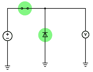
This setup hardly has any voltage drop, but this is not quite as easy to implement as the previous ideas. You need to install the fuse in an easily accessible place, and the “crowbar” diode current rating must be greater than the fuse. You can use a resettable fuse instead of the usual fuse, but you will often need to buy them in bulk!
- IN4007 Datasheet https://www.vishay.com/docs/88503/1n4001.pdf
- 1N5817 Datasheet https://www.vishay.com/docs/88525/1n5817.pdf
- Resettable Fuse Selection Guide (unbiased) https://www.rutronik.com/fileadmin/Rutronik/Downloads/printmedia/products/03_electromechanical/littelfuse_resettable_fuses_en.pdf
The P-Channel MOSFET Trick
This is another simple and easy-to-implement idea that introduces a very low voltage drop. The clever trick is to add a P-channel Power MOSFET on the high side of a circuit which only allows power to flow when the polarity of the source voltage is correct!
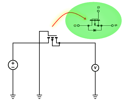
At this point note that the MOSFET is actually wired in the reverse orientation as it would normally – the Drain and Source terminals are reversed. This is intentional and is necessary so that the slight leakage current through the MOSFET’s intrinsic body diode will bias the MOSFET on only when the polarity is correct.
As shown in the basic scheme above, the Gate of the MOSFET is hooked to ground rail, allowing current to move across the Drain-Source junction when the power source is connected. You can also use a zener diode to keep the gate voltage within a safe range (see below). The Zener diode voltage, however, must be less than the MOSFET VGS – The maximum voltage allowed from Gate to Source. Additionally, it must be higher than the MOSFET VGS(th) – the threshold voltage from Gate to Source.
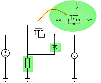
Look, if the supply voltage is less than the maximum gate to source voltage (Vgs) of the MOSFET, you only need the MOSFET (just connect the gate directly to ground). While reading your MOSFET’s datasheet, if you find the maximum Vgs could exceed the Vcc level, then you must clamp the voltage between the gate and the source using the zener diode-resistor combination. By inserting a zener diode with a voltage less than the maximum Vgs, you can limit the voltage between the gate and the source to a safe level. Nevertheless, the associated resistor (10K to 100K) must provide ample current to properly bias the zener diode chosen by you, that means it can feed the minimum current required to achieve the zener breakdown voltage.
Now to a few key things you should know about MOSFETs and Zener Diodes:
MOSFET
- VDS: Voltage Drain to Source – This must be greater than the power supply voltage/Vcc
- RDS(on): Resistance of the Drain to Source when the MOSFET is turned on – This must be as low as possible
- VGS: Gate-Source Voltage – This is the maximum voltage allowed from Gate to Source
- VGS(th): The voltage at which the MOSFET will turn on to “some” degree
Zener Diode
- Zener knee: At a certain voltage in reverse bias condition, the reverse breakdown occurs and current increases rapidly. This sharp change in zener current is called as knee or zener knee of the reverse characteristics
- Zener Breakdown Voltage: The reverse bias voltage at which the breakdown occurs is called zener breakdown voltage, denoted as V
- Izmin and Izmax: Izmin is minimum current through the zener diode to maintain its operation while Izmax is maximum current allowed to flow through the zener diode
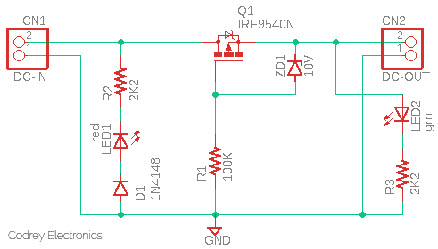
DIY Reverse Voltage Defender (Version 1)
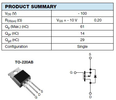
The following circuit can be used as a reverse voltage defender. This is a practical implementation of the aforesaid P-Channel MOSFET trick, now with a quite popular P-channel Power MOSFET – the IRF9540 (https://www.vishay.com/docs/91078/91078.pdf).
For a given load current, the low on-resistance of the MOSFET drops much less voltage than that of an equivalent bipolar junction transistor (BJT). The result is lower power dissipation (I2R), which enables the MOSFET to handle much higher load currents than are possible with a BJT of the same size.
In the below datasheet snip, you can see that the maximum on-resistance of IRF9540 MOSFET is only 0.20Ω (at -10V VGS). So, the wasted power in case of a 1A current flow will be around RDS(on) x I2 = 0.2Ω x 1A x 1A = 200mW only!
Understanding Power MOSFET Parameters https://www.taiwansemi.com/assets/uploads/productcategoryfile/AN-1001_A1611.pdf
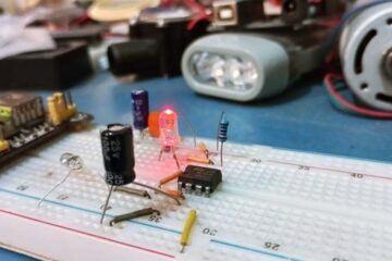
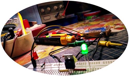
As usual, I tested this concept on a breadboard using 12VDC/1A input. Just a sanity check, that’s it.
Remember to pay careful attention to the MOSFET’s orientation in this circuit. The MOSFET is wired as a high-side switch, so its body diode should be oriented in the direction of normal current flow. Then, a reversed voltage input reverse-biases the diode and blocks the flow of current. Also, it is a good idea to use a heat sink with the MOSFET in your final construction.
Recommended: AiPCBA PCB Assembly Manufacturing Service 20% OFF For Parts, Turnkey PCBA Prototype Online, BOM Online 30s quick Quoting
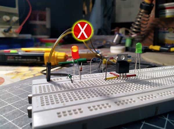
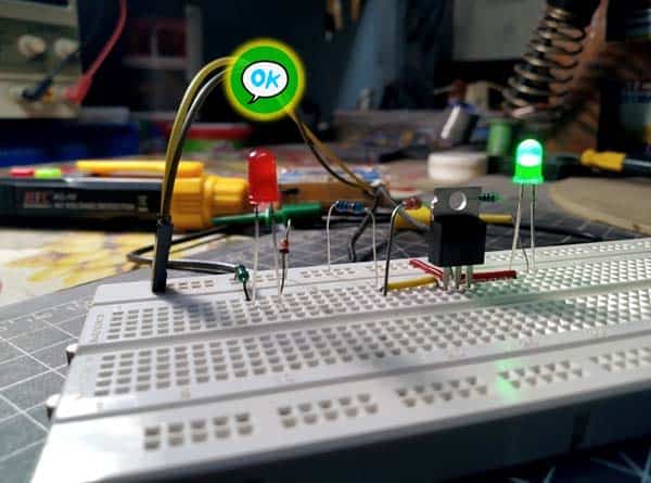
The 2-pin connector CN1 is the input port of this circuit while CN2 is the output port. The red LED1 is a simple reverse polarity input annunciator, and the green LED 2 is the output status indicator.
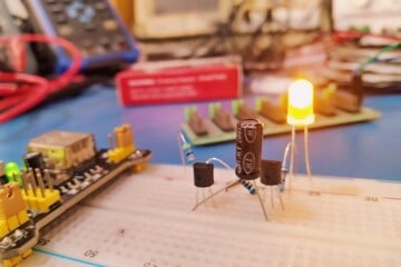
More breadboard snaps. All is good!
Keep an eye open, for power sources/battery voltages lower than 10V but higher than 2.7V, you can use a low-voltage P-Channel MOSFET. Another is the application of a low-threshold device with a charge pump for driving its gate voltage below ground. I know this has been covered by somebody in detail – Google is your best friend (https://giybf.com/)!
Cheerful Betterment Thoughts
There’s another thing that works great here – reverse polarity protection smart diode controllers!
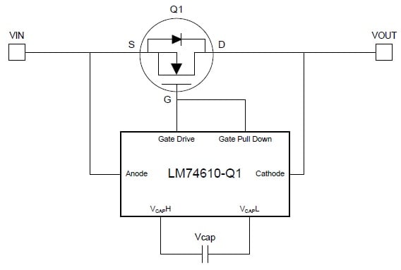
I’ve been interested in specialized ICs for reverse voltage protection for a while myself. The LM74610-Q1 is a good chip I found while searching the Internet (https://www.mouser.in/new/texas-instruments/ti-lm74610-q1-controller/).
The LM74610-Q1 (https://www.ti.com/lit/ds/symlink/lm74610-q1.pdf) is a dedicated controller device that can be used with an N-Channel MOSFET in a reverse polarity protection circuitry. See, often NMOS FETs are more attractive than PMOS FETs for high-current applications – https://www.maximintegrated.com/en/design/technical-documents/app-notes/6/636.html.
The LM74610-Q1 is designed to drive an external MOSFET to emulate an ideal diode rectifier when connected in series with a power source. The unique advantage here is that the controller is not referenced to ground and thus has Zero IQ, that means the device draws zero steady-state quiescent current from the supply. More about IQ https://www.ti.com/lit/an/slyt412/slyt412.pdf
Likewise, I happen to stumble upon the IC Chip VN5R003H-E, which is a device made by ST to provide reverse battery protection to an electronic module. This is the datasheet of that 3mΩ reverse battery protection switch https://www.st.com/resource/en/datasheet/vn5r003h-e.pdf
A careful discussion about these pretty useful chips is outside the scope of this little blog post. However, there are several online resources available that provide above-average treatment of the topic. You can (hopefully) learn more about them through other media sites on the Aspencore network (https://aspencore.com/media/).
Stopping Point
Now towards the last line of a long (perhaps boring) explanation of what reverse voltage protection is, how it works, and how to design/build simple circuits to make devices resistant to power sources connected backward. As before, if you have a doubt or query post it in the comments below. I am also interested to have your suggestions about the reverse voltage protection tricks. Thanks for reading and I hope I have helped some novices.